Light-emitting diode epitaxial wafer and manufacturing method thereof

A technology of light-emitting diodes and epitaxial wafers, applied in the direction of electrical components, circuits, semiconductor devices, etc., can solve the problems of low light-emitting efficiency of light-emitting diodes, and achieve the effects of facilitating lateral expansion, avoiding interface polarization, and improving effective doping

Inactive Publication Date: 2017-09-05
HC SEMITEK ZHEJIANG CO LTD
View PDF13 Cites 7 Cited by
  • Summary
  • Abstract
  • Description
  • Claims
  • Application Information

AI Technical Summary

Problems solved by technology

[0006] In order to solve the problem of low luminous efficiency of light-emitting diodes in the prior art, an emb...

Method used


Image

  • Light-emitting diode epitaxial wafer and manufacturing method thereof
  • Light-emitting diode epitaxial wafer and manufacturing method thereof
  • Light-emitting diode epitaxial wafer and manufacturing method thereof

Examples


Embodiment 1

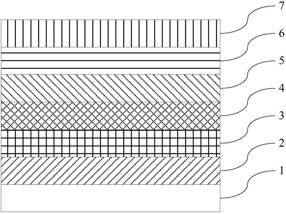
[0033] An embodiment of the present invention provides an epitaxial wafer of a light emitting diode, see figure 1 , the epitaxial wafer includes a substrate 1 and a buffer layer 2, an undoped gallium nitride layer 3, an N-type gallium nitride layer 4, a multi-quantum well layer 5, an electron blocking layer 6 and a P type GaN layer 7 .

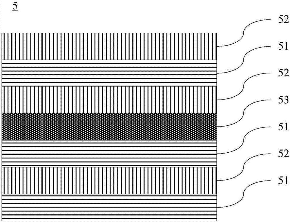
[0034] In this example, see figure 2 The multi-quantum well layer 5 includes a plurality of quantum wells 51 and a plurality of quantum barriers 52, the plurality of quantum wells 51 and the plurality of quantum barriers 52 are alternately stacked, and the quantum wells are InGaN layers. Multi-quantum well 5 also comprises at least one graphene film layer 53, and graphene film layer 53 is arranged between two adjacent quantum wells 51 and quantum barrier 52, when the quantity of graphene film layer 53 exceeds 1, phase At least one quantum well 51 or at least one quantum barrier 52 ( figure 2 Only take one graphene film layer as an example...

Embodiment 2

[0056] An embodiment of the present invention provides an epitaxial wafer of a light emitting diode, and the epitaxial wafer provided in this embodiment is a specific implementation of the epitaxial wafer provided in Embodiment 1.

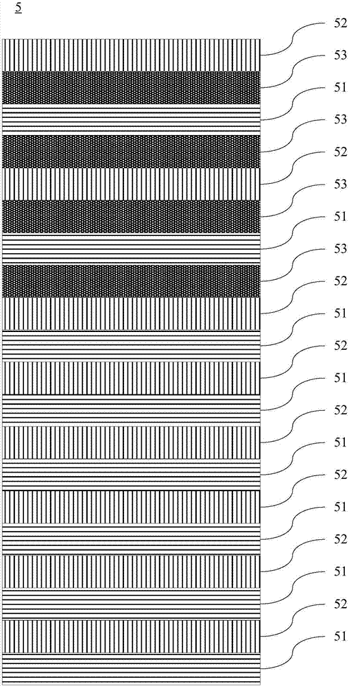
[0057] In this example, if image 3 As shown, the multi-quantum well layer 5 includes 8 quantum wells 51 and 8 quantum barriers 52, and the junctions between each quantum well 51 and the adjacent quantum barrier 52 in the two quantum wells 51 closest to the electron blocking layer 6 are all provided. There is a graphene film layer 53 .

[0058] Experiments have found that the epitaxial wafer of the present embodiment is comparable to the traditional epitaxial wafer (the multi-quantum well layer includes 8 quantum wells and 8 quantum barriers, and the junction of each quantum well and the adjacent quantum barrier is not provided with a graphene film layer). ratio, the current density is 50A / cm 2 When the luminous efficiency is increased by 2%, the...

Embodiment 3

[0060] An embodiment of the present invention provides an epitaxial wafer of a light emitting diode, and the epitaxial wafer provided in this embodiment is another specific realization of the epitaxial wafer provided in Embodiment 1.

[0061] In this example, if Figure 4 As shown, the multi-quantum well layer 5 includes 8 quantum wells 51 and 8 quantum barriers 52, and the graphene film layer 53 is arranged at the junction of the quantum wells 51 and the quantum barriers 52, and between adjacent graphene film layers 53 Two quantum wells 51 and two quantum barriers 52 are provided.

[0062] Experiments have found that the epitaxial wafer of the present embodiment is comparable to the traditional epitaxial wafer (the multi-quantum well layer includes 8 quantum wells and 8 quantum barriers, and the junction of each quantum well and the adjacent quantum barrier is not provided with a graphene film layer). ratio, the current density is 50A / cm 2 When the luminous efficiency is in...


PUM

PropertyMeasurementUnit
Thicknessaaaaaaaaaa
Growth temperatureaaaaaaaaaa
Growth pressureaaaaaaaaaa

Abstract

The invention discloses a light-emitting diode epitaxial wafer and a manufacturing method thereof, which belong to the technical field of semiconductors. The epitaxial wafer comprises a substrate, a buffer layer, an un-doped gallium nitride layer, an N-type gallium nitride layer, a multi-quantum well layer, an electron barrier layer and a P-type gallium nitride layer, wherein the multi-quantum well layer comprises multiple quantum wells and multiple quantum barriers; the multiple quantum wells and the multiple quantum barriers are arranged in an alternately-stacked mode; the quantum well is an indium gallium nitride layer; the multi-quantum well layer also comprises at least one graphene film layer; each graphene film layer is arranged between the quantum well and the adjacent quantum barrier respectively; and when the number of graphene film layers is larger than one, at least one quantum well or at least one quantum barrier is arranged between adjacent two graphene film layers. The effective doping of indium in the quantum well can be improved, high temperature can be adopted to grow the quantum well, the quantum well growth quality is improved, interfacial polarization is improved, and the light-emitting efficiency of the light-emitting diode is improved.

Description

technical field [0001] The invention relates to the technical field of semiconductors, in particular to an epitaxial wafer of a light emitting diode and a preparation method thereof. Background technique [0002] Light Emitting Diode (English: Light Emitting Diode, referred to as: LED) is a semiconductor light emitting device made by using the principle of semiconductor PN junction electroluminescence. The epitaxial wafer is the primary product in the process of manufacturing light-emitting diodes. [0003] The existing epitaxial wafer includes a sapphire substrate and a buffer layer, an undoped gallium nitride layer, an n-type gallium nitride layer, a multi-quantum well layer, an electron blocking layer and a p-type gallium nitride layer stacked on the sapphire substrate in sequence. layer. Wherein, the multi-quantum well layer includes multiple quantum wells and multiple quantum barriers, the multiple quantum wells and multiple quantum barriers are alternately stacked, t...

Claims


Application Information

Patent Timeline
IPC IPC(8): H01L33/06H01L33/32H01L33/00
CPCH01L33/06H01L33/007H01L33/325
Inventor 王群郭炳磊董彬忠李鹏王江波
Owner HC SEMITEK ZHEJIANG CO LTD
Why Eureka
Try Eureka