
Fast time response semiconductor radiation detector and manufacturing method thereof

A radiation detector and time-response technology, applied in radiation measurement, radiation intensity measurement, X/γ/cosmic radiation measurement, etc., can solve signal carrier transport time extension, time response curve tailing, time response Problems such as characteristic differences, to achieve the effect of improving time response characteristics, solving the problem of trailing edge tailing, and fast time response characteristics

Active Publication Date: 2019-06-07
NORTHWEST INST OF NUCLEAR TECH
View PDF4 Cites 0 Cited by
  • Summary
  • Abstract
  • Description
  • Claims
  • Application Information

AI Technical Summary

Problems solved by technology

Under the condition of high-intensity pulsed ray incidence, a large number of signal carriers are generated in the crystal, which are captured and decaptured by a large number of carrier traps in the CZT crystal during the transport process, and the signal carriers trapped by the traps The transit time is extended, and the tailing phenomenon of the falling edge appears on the time response curve of the CZT detector, making it difficult to obtain the time information of the pulsed ray source from the time response curve of the detector
[0007] Due to the trapping and decapturing effects of defects in the crystal on the signal carrier, the uncertainty of crystal quality makes the time response performance of different single crystal CZT detectors have great differences. Along with the tailing problem, on the other hand, it also increases the difficulty of constructing the theoretical model of the CZT detector. There are differences between the constructed model and the actual CZT detector time response characteristics

Method used


Image

  • Fast time response semiconductor radiation detector and manufacturing method thereof
  • Fast time response semiconductor radiation detector and manufacturing method thereof
  • Fast time response semiconductor radiation detector and manufacturing method thereof

Examples


Embodiment Construction

[0037] The present invention will be further described below in conjunction with the accompanying drawings and specific embodiments.

[0038] This embodiment takes a CZT detector as an example, and is also applicable to detectors of other types of crystals.

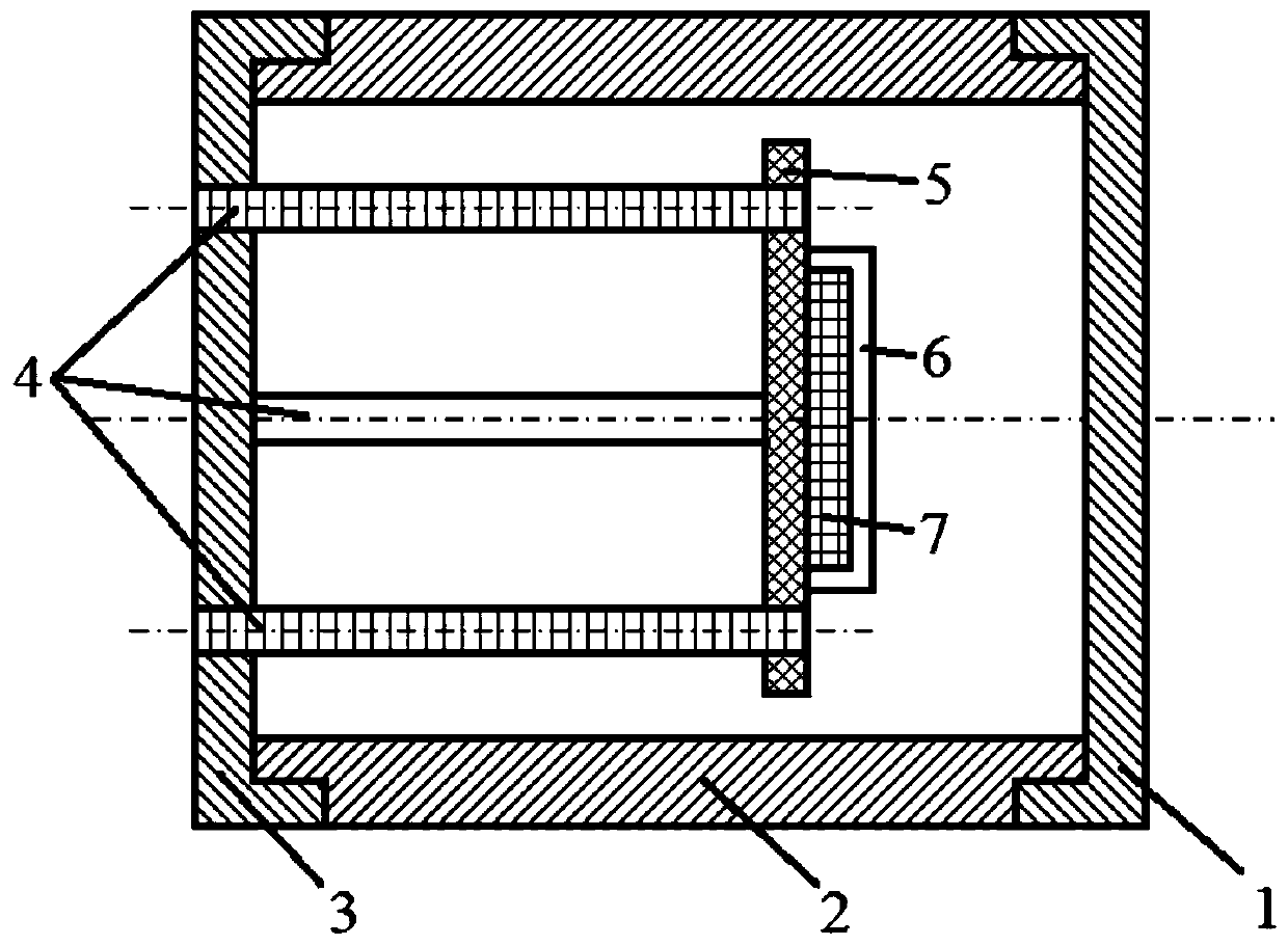
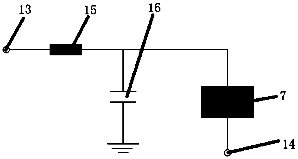
[0039] Such as Figure 4 As shown, the cadmium zinc telluride (CdZnTe, referred to as CZT) detector with fast time response in this embodiment includes a sealed casing formed by sequentially connecting the front cover 1, the middle tube 2 and the rear cover 3 and the signal signal set inside the casing. The material of the output circuit 12, semiconductor components and semiconductor diode 21 is Fe, and the inside is evacuated or filled with inert gas.

[0040] The semiconductor assembly includes a substrate 5, a CZT single crystal 7 glued on the substrate 5 by a sealing glue 6 through a sealing process, a collecting electrode layer 9 and a high-voltage electrode layer 8 respectively arranged on the front and rear end fa...


PUM


Abstract

The invention relates to a radiation detection device, particularly to a fast-time-response semiconductor radiation detector based on shortwave light injection and a method of manufacturing the same. The semiconductor radiation detector comprises a detector body including a detector front cover and a semiconductor crystal. And the semiconductor radiation detector also includes a shortwave light source arranged at the inner side wall of the detector front cover; the shortwave light source points to the center of the semiconductor crystal; and the emission angle of the shortwave light source covers the whole semiconductor crystal space region and the central wavelength of the shortwave light source is shorter than that corresponding to a semiconductor crystal energy gap. Therefore, the influence on the time response characteristic of the detector by the crystal quality can be eliminated; and a noel CZT detector having a fast time response characteristic is provided for pulse radiation field measurement.

Description

technical field [0001] The invention relates to a radiation detection device, in particular to a semiconductor radiation detector with fast time response based on short-wave light injection. Background technique [0002] Cadmium zinc telluride (CdZnTe, referred to as CZT) is a new room temperature compound semiconductor material, which has comprehensive advantages such as high average atomic number, high density, high resistivity and wide band gap. [0003] The high average atomic number enables the CZT detector to have a high detection efficiency for medium and high energy X / γ-rays; the high density makes the CZT detector small in size and has strong compatibility in group detection and space detection. Great advantages; high resistivity and wide bandgap width, so that the CZT detector has a lower dark current at room temperature, which solves the low-temperature application limitations of commonly used Si and Ge semiconductor radiation detectors, and effectively reduces th...

Claims


Application Information

Patent Timeline
Patent Type & Authority Patents(China)
IPC IPC(8): G01T1/24
CPCG01T1/24G01T1/241
Inventor 韩和同陈翔傅录祥宋朝晖管兴胤张子川刘君红李刚卢毅
Owner NORTHWEST INST OF NUCLEAR TECH
Learn More