

Organic semiconductor material composition and semiconductor layer of organic field effect transistor and preparation method for semiconductor layer
A material composition and organic semiconductor technology, applied in the manufacture/processing of organic semiconductor devices, semiconductor/solid-state device manufacturing, semiconductor devices, etc., can solve the problem of inability to prepare organic field effect transistor devices, limit the wide application of related devices, and make it difficult to realize Large-area preparation and other issues, to achieve the effect of improving production efficiency and production scale, good crystallization performance, and improving performance
Inactive Publication Date: 2017-09-15
SHANGHAI MI FANG ELECTRONICS LTD
View PDF2 Cites 4 Cited by
- Summary
- Abstract
- Description
- Claims
- Application Information
AI Technical Summary
Problems solved by technology
[0005] Existing n-type semiconductor materials cannot meet the process requirements of fully printed OFETs that can be printed in air and post-processed, so it is difficult to achieve large-area fabrication. In addition, existing n-type semiconductor materials cannot be fabricated on flexible substrates. Airport effect transistor devices, which limit the wide application of related devices
Method used
View moreImage
Smart ImageViewing Examples

Examples
Embodiment 1
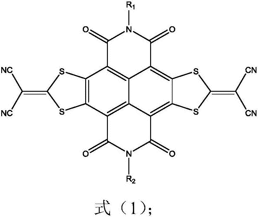
[0052] This example is used to illustrate the organic semiconductor material composition of the present disclosure.
[0053] Take 5 mg of NDI3HU-DTYM2, 1 mg of polymer polystyrene (brand name: BCBS8212V, weight average molecular weight: 560,000) and 1 mL of solvent 1,3,5-trimethylbenzene, mix them thoroughly, and obtain the organic semiconductor material composition of this embodiment.
Embodiment 2-8
[0055] The composition and content of the organic semiconductor material composition are shown in Table 1, and the organic semiconductor material compositions of Examples 2-8 were prepared by the steps of Example 1 respectively.
[0056] Wherein, in Example 8, the grade of polystyrene is MKBQ8943V, and the weight average molecular weight is 5,000.
Login to View More PUM
 Abstract
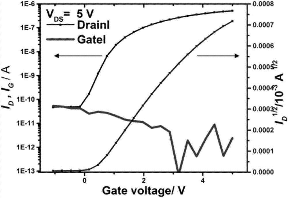
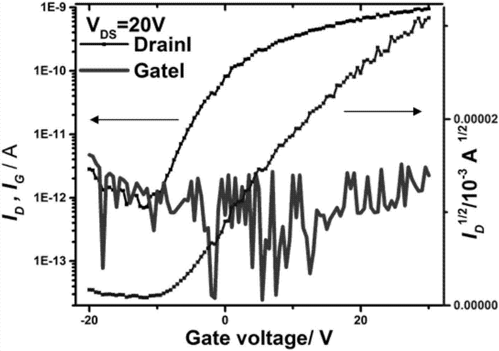
The invention relates to an organic semiconductor material composition and a semiconductor layer of an organic field effect transistor and a preparation method for the semiconductor layer. The organic semiconductor material composition comprises a naphthalimide derivative, a polymer additive and an organic solvent. The organic semiconductor material composition disclosed in the invention can prepare the semiconductor layer of the organic field effect transistor by adopting film dropping or ink jetting and printing methods, so that preparation of the organic field effect transistor by adopting an all-soliton method or even an all-printing method can be realized, and production efficiency and production scale can be improved and enlarged; and in addition, the composition is high in stability in the air, the prepared semiconductor layer is high in crystallization property, the performance of the transistor can be improved, and operation of the organic field effect transistor at a low voltage (less than or equal to 5V) can be realized. Particularly, the semiconductor composition disclosed in the invention adopts the non-chlorine solvent which has relatively low pollution to environment and human body, so that the chlorine-containing solvent which cannot be degraded by microbe in environment easily and is commonly used in the existing organic semiconductor field can be replaced.
Description
technical field [0001] The present disclosure relates to organic electronic devices, in particular, to an organic semiconductor material composition, a semiconductor layer of an organic field effect transistor and a preparation method thereof. Background technique [0002] Organic field-effect transistor (Organic Thin Film Transistor, OFET) has aroused people's general interest because of its wide application prospect, low cost and convenient preparation. OFET is composed of electrodes (source, drain, gate), insulating layer and organic semiconductor layer. At present, the electrode part of OFET is mostly prepared by vacuum evaporation method, the insulating layer is mostly prepared by spin coating method, and the semiconductor layer is mostly prepared by droplet coating. film or spin-coating process. [0003] Organic semiconductors are an important part of OFETs. According to the type of transport carriers, organic semiconductors are divided into n-type materials that tran...
Claims
Login to View More Application Information
Patent Timeline
 Patent Type & AuthorityApplications(China)
IPC IPC(8): H01L51/05H01L51/30
CPCH10K85/00H10K85/657H10K10/46H10K71/00
Inventor高思敏
OwnerSHANGHAI MI FANG ELECTRONICS LTD