Semiconductor device and method for manufacturing same
What is AI technical title?
AI technical title is built by Patsnap AI team. It summarizes the technical point description of the patent document.
a technology of semiconductor devices and semiconductors, applied in semiconductor devices, semiconductor/solid-state device details, electrical apparatus, etc., to achieve the effect of preventing the attachment of die-bonding materials, increasing on resistance, and facilitating leakage failures in a order
Inactive Publication Date: 2013-01-10
RENESAS ELECTRONICS CORP
View PDF0 Cites 20 Cited by
Summary
Abstract
Description
Claims
Application Information
AI Technical Summary
This helps you quickly interpret patents by identifying the three key elements:
Problems solved by technology
Method used
Benefits of technology
Benefits of technology
The invention relates to a method for applying a die-bonding material to a wiring board to improve the production of semiconductor devices. The method aims to prevent leakage of the die-bonding material and to avoid the formation of a dam between the chip and the bonding lead. The invention also focuses on the thinning of the chip to suppress the overall thickness of the semiconductor package and to reduce the ON resistance of power transistors. Additionally, the invention provides a technique for applying the die-bonding material without excessive wet spread during the chip mounting process. These technical effects contribute to the improved production efficiency and reliability of semiconductor devices.
Problems solved by technology
However, above-described Patent Documents do not describe technique of solving a problem upon mounting a thinned semiconductor chip on a lead frame or wiring board, that is, crawling up of a part of a die-bonding material that leaked to the outside from a lower surface to an upper surface of the semiconductor chip.
Method used
Image
Click on the blue label to locate the original text in one second.
Reading with bidirectional positioning of images and text.
Examples
first embodiment
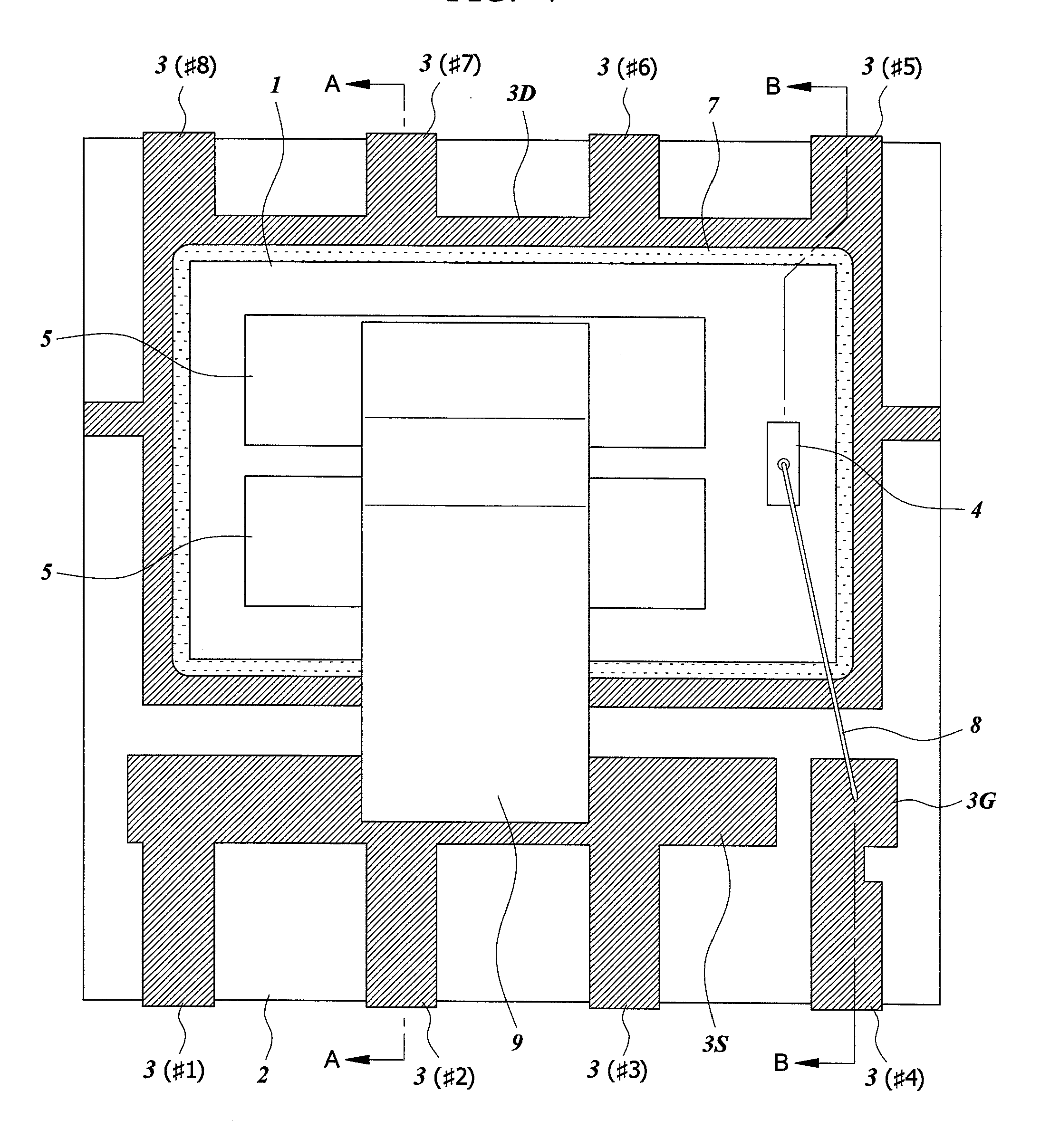
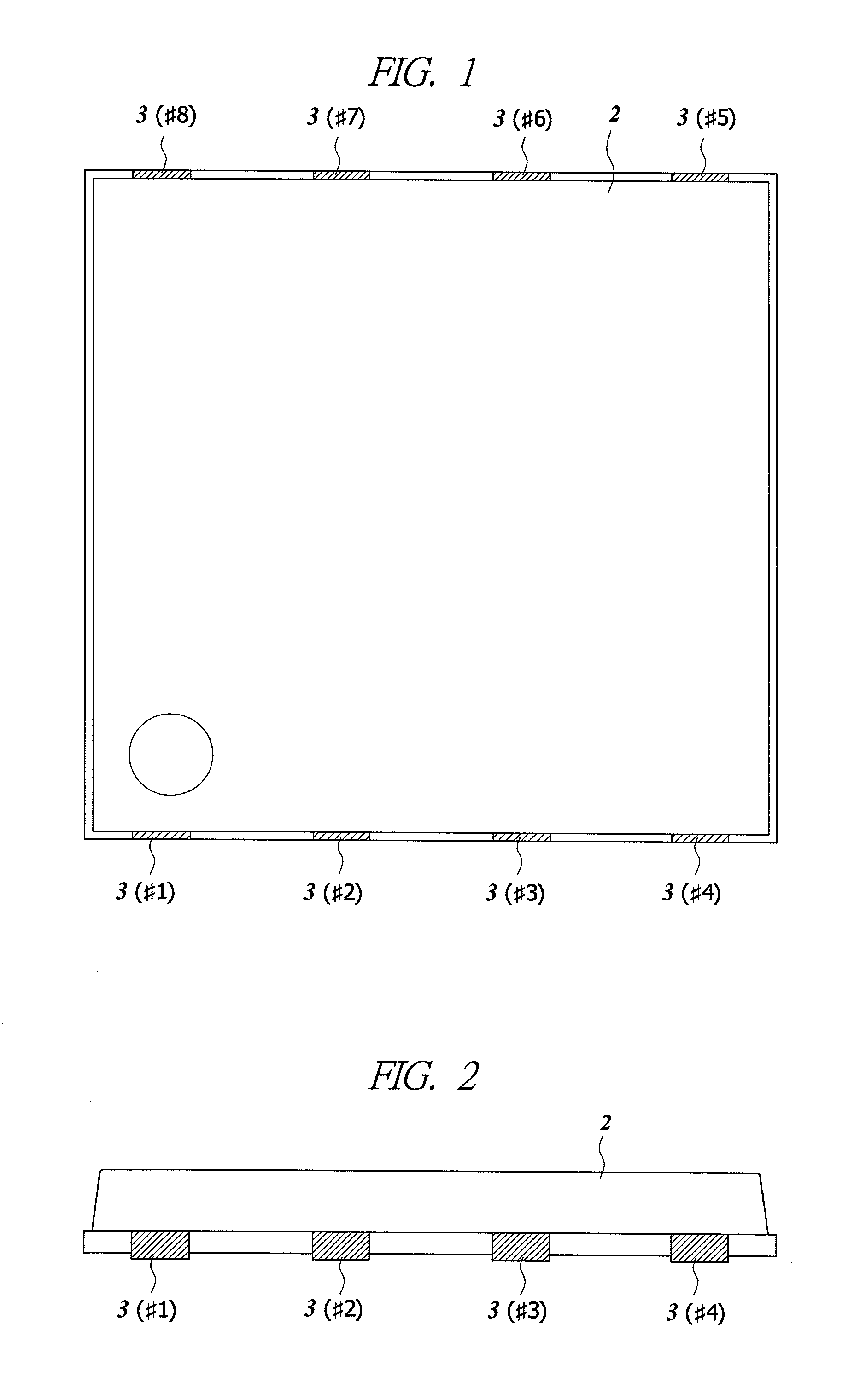
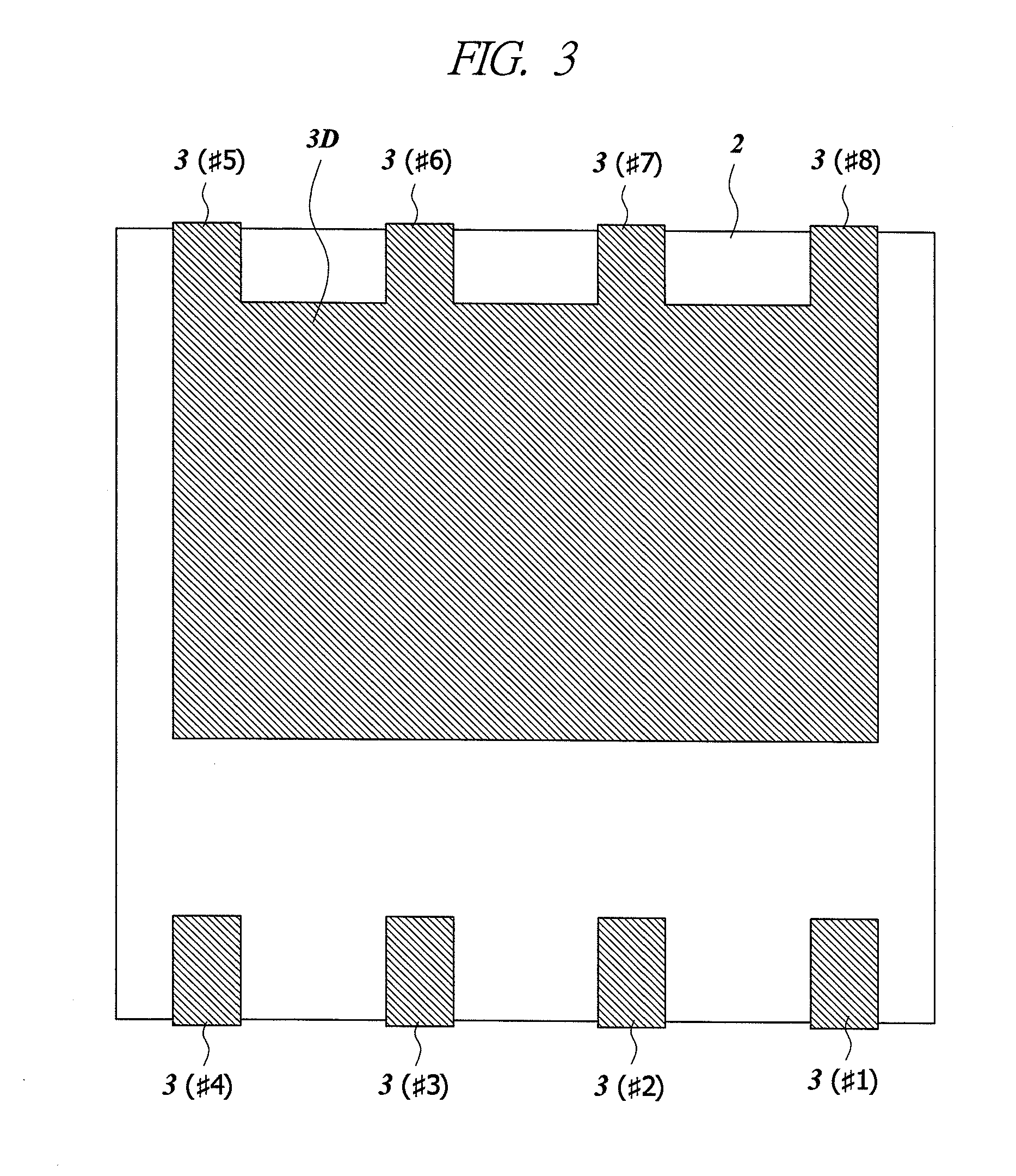
[0118]FIGS. 1 to 5 are diagrams illustrating a semiconductor device of the present embodiment, in which FIG. 1 is a planar view, FIG.
[0119]2 is a side view, FIG. 3 is a planar view illustrating a back surface (substrate mounting surface), FIG. 4 is a planar view illustrating an inner structure, FIG. 5 is a cross-sectional view along the line A-A in FIG. 4, and FIG. 6 is a cross-sectional view along the line B-B in FIG. 4.
[0120]The semiconductor device of the present embodiment is a small surface-mountpackage (called FLP: Flat Lead Package) in which a chip 1 mounted on a die pad (chip mounting portion) 3D of a lead frame is sealed by a mold resin 2, and eight leads 3 (#1 to #8) composing external connection terminals of the semiconductor device are exposed in two side surfaces and a back surface (substrate mounting surface) of the mold resin 2. In addition, in the back surface of the mold resin 2, for diffusing heat generated in the chip 1 and reducing thermal resistance of the pack...
second embodiment
[0213]The method of applying a die-bonding material onto a die pad of a lead frame using the stamping nozzle 42 described above is applicable to manufacturing of a small surface-mountpackage in which a plurality of chips are mounted on a die pad.
[0214]FIG. 51 is a planar view illustrating an inner structure of a semiconductor device of the present embodiment, and FIG. 52 is an inner equivalent circuit diagram of the semiconductor device. The semiconductor device of the present embodiment is a small surface-mountpackage in which two chips 1H and 1L are sealed with a mold resin 2. Various shapes such as FLP, SOP8 described above and so forth can be adopted as a shape of the package.
[0215]To a main surface of the chip 1H having a smaller diameter size of the two chips 1H and 1L, a high-side MOSFET is formed; and, to a main surface of the chip 1L having a larger diameter size, a low-side MOSFET is formed. Thicknesses of the two chips 114 and 1L are both, for example, 100 lam or smalle...
third embodiment
[0232]While the semiconductor device mounting a chip in a chip mounting portion (die pad) of a lead frame has been described in the first and second embodiments, the present invention is applicable to a semiconductor device mounting a chip in a chip mounting portion of a wiring board.
[0233]FIGS. 55A and 55B illustrate a BGA type semiconductor device mounting a chip 1M to which a multi-pin integrated circuit such as a microcomputer on a wiring board 17.
[0234]To an upper surface of the wiring board 17 to be a relay board (interposer) for connecting the chip 1M to a mother board of electronic parts, the chip 1C is mounted via the insulating paste 15 described above. In a peripheral portion of a main surface of the chip 1C, the plurality of electrode pads (bonding pads) 16 are formed, and, in a peripheral portion of an upper surface of the wiring board 17, a plurality of bonding leads 18 are formed. In addition, the electrode pads 16 of the chip 1C and the bonding leads 18 of the wiring...
PUM
Abstract
A dug portion (50) in which a die-bonding material is filled is provided to a lower surface of a stampingnozzle (42) used in a step of applying the die-bonding material onto a chip mounting portion of a wiring board. Planar dimensions of the dug portion (50) are smaller than external dimensions of a chip to be mounted on the chip mounting portion. In addition, a depth of the dug portion (50) is smaller than a thickness of the chip. When the thickness of the chip is 100 μm or smaller, a problem of crawling up of the die-bonding material to an upper surface of the chip is avoided by applying the die-bonding material onto the chip mounting portion using the stampingnozzle (42).
Description
TECHNICAL FIELD[0001]The present invention relates to a semiconductor device and a method of manufacturing the same and more particularly relates to technique effectively applied to a semiconductor device in which a semiconductor chip is mounted on a wiring board using a paste-like die-bond material and a method of manufacturing the semiconductor device.BACKGROUND ART[0002]Patent Document 1 (Japanese Patent Application Laid-Open Publication No. 2007-149784) discloses a solder supplying apparatus having a nozzle at a lower portion of a crucible of a sealed container structure and discharges a liquid solder for die-bonding accommodated on the crucible on a stamping basis. The crucible includes solder heating means for heating a solid solder to be a liquid solder, discharge control means which controls switching of positive pressure and negative pressure of the inner pressure of the crucible, a fluid level sensor which detects volume of the liquid solder, and solder replenish means whi...
Claims
Application Information
Patent Timeline
Application Date:The date an application was filed.
Publication Date:The date a patent or application was officially published.
First Publication Date:The earliest publication date of a patent with the same application number.
Issue Date:Publication date of the patent grant document.
PCT Entry Date:The Entry date of PCT National Phase.
Estimated Expiry Date:The statutory expiry date of a patent right according to the Patent Law, and it is the longest term of protection that the patent right can achieve without the termination of the patent right due to other reasons(Term extension factor has been taken into account ).
Invalid Date:Actual expiry date is based on effective date or publication date of legal transaction data of invalid patent.
Patent Type & AuthorityApplications(United States)

