A kind of bcd device and its manufacturing method
A manufacturing method and device technology, applied in the field of BCD devices and their manufacturing, can solve the problems of size reduction, cost increase, unfavorable cost savings, etc., and achieve the effects of increasing the number, reducing device loss, and improving competitiveness.
- Summary
- Abstract
- Description
- Claims
- Application Information
AI Technical Summary
Problems solved by technology
Method used
Image

Examples
Embodiment 1
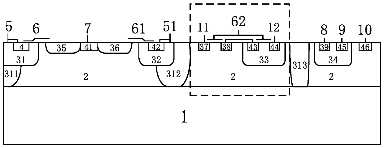
[0039] Figure 4 Shown is a schematic diagram of the structure of a BCD device of the present invention, its cell structure includes a substrate 1, a first epitaxial layer 2, a second epitaxial layer 21, a first P isolation 311, a second P isolation 312, and a third P isolation 313, the first P well 31, the third P well 33, the fourth P well 34, the DMOS source P-type heavily doped region 310, the third P-type heavily doped region 37, and the fourth P-type heavily doped region 38 , the fifth P-type heavily doped region 39, the DMOS source N-type heavily doped region 4, the DMOS drain N-type heavily doped region 41, the second N-type heavily doped region 43, the third N-type heavily doped region Region 44, the fourth N-type heavily doped region 45, the fifth N-type heavily doped region 46, the DMOS source electrode 5, the contact electrode 51 of the first P well 31, the DMOS gate electrode 6, the PMOS gate electrode 62, the NMOS gate electrode Electrode 63, PMOS source electro...
Embodiment 2
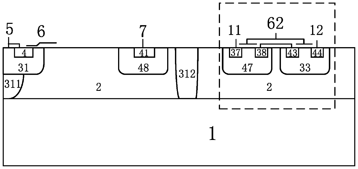
[0053] like image 3 As shown, this embodiment is basically the same as Embodiment 1, and the main difference is that the BCD device further includes a P Type doped region 314 , the upper surface of which is tangent to the upper surface of the second epitaxial layer 21 .
[0054] The manufacturing method of the above-mentioned BCD device is basically the same as the manufacturing method in Embodiment 1, the difference is that after the second epitaxial layer 21 is grown, P-type impurity ions are implanted to form a P-type doped region 314, so that its upper surface is in contact with the second epitaxial layer 21. The upper surface of the epitaxial layer 21 is tangential.
Embodiment 3
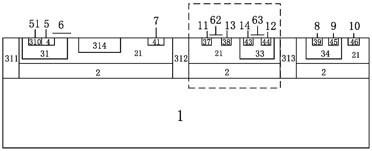
[0056] like Figure 5 As shown, this embodiment is basically the same as Embodiment 2, the main difference is that the P-type doped region 314 arranged between the first P well 31 and the N-type heavily doped region 41 of the DMOS drain, on which The surface is not tangent to the upper surface of the second epitaxial layer 21 .
[0057] The manufacturing method of the above-mentioned BCD device is basically the same as the manufacturing method in Example 1, the difference is that: P-type impurity ion implantation is performed before the growth of the second epitaxial layer 21 to form a P-type doped region 314, so that its upper surface is not in contact with the second epitaxial layer 21. The upper surfaces of the two epitaxial layers 21 are tangent to each other.
PUM
 Abstract
Description
Claims
Application Information
 - R&D
- Intellectual Property
- Life Sciences
- Materials
- Tech Scout
- Unparalleled Data Quality
- Higher Quality Content
- 60% Fewer Hallucinations
Browse by: Latest US Patents, China's latest patents, Technical Efficacy Thesaurus, Application Domain, Technology Topic, Popular Technical Reports.
© 2025 PatSnap. All rights reserved.Legal|Privacy policy|Modern Slavery Act Transparency Statement|Sitemap|About US| Contact US: help@patsnap.com