

Plasmon nanometer structure-based tunable random laser array device
A nanostructure and random laser technology, which is applied to laser parts, lasers, laser devices, etc., can solve the problems of high laser threshold and non-tunable directionality, and achieve high beam quality
Active Publication Date: 2017-09-29
SOUTHEAST UNIV
View PDF8 Cites 14 Cited by
- Summary
- Abstract
- Description
- Claims
- Application Information
AI Technical Summary
Problems solved by technology
[0007] Technical problem: The purpose of this invention is to solve the bottleneck problems of existing random lasers such as high laser threshold, radiation spectrum, and non-tunable directivity.
Method used
View moreImage
Smart ImageViewing Examples

Examples
example
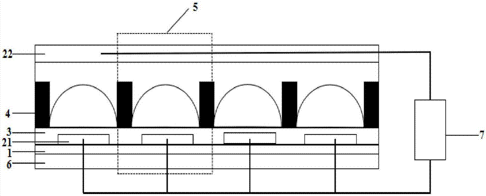
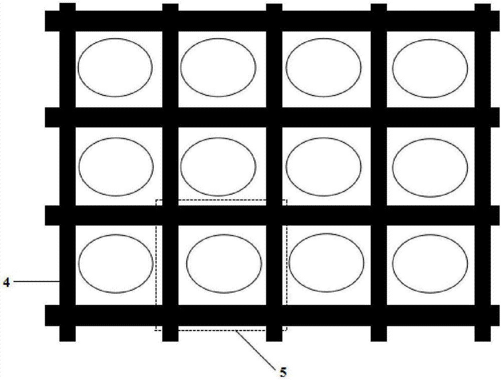
[0037] Such as figure 1 A laser array structure of M×N is prepared as shown, and a transparent electrode is prepared on the substrate by photolithography, etching and other processes, and then a dielectric layer is prepared by ALD on top, and a low surface stress polymer dielectric layer is prepared by a spin-coating process. Subsequently, an M×N grid layer is prepared by nanoimprinting technology to form an array chamber structure.
Login to View More PUM
| Property | Measurement | Unit |
|---|---|---|
| Thickness | aaaaa | aaaaa |
Abstract
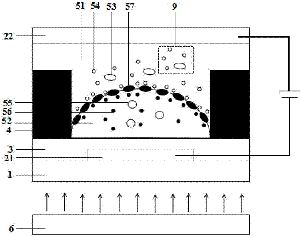
The invention discloses a plasmon nanometer structure-based tunable random laser array device. The random laser array device sequentially comprises a pumping light source (6), a substrate (1), a bottom electrode (21), a dielectric layer (3), a laser cavity unit (5) and a top electrode (22) from bottom to top, the laser cavity unit (5) is encircled by a spacing layer (4), and an peripheral driving circuit (7) forms a closed loop by the bottom electrode (21) and the top electrode (22). By the tunable random laser array device, two light sources can be obtained: conventional lighting light and random laser; rapid switch between the two light sources is achieved by changing a working voltage; and moreover, compared with existing random laser devices, the obtained random laser has the advantages of low threshold, dynamic direction tunability, high efficiency and the like.
Description
technical field [0001] The invention belongs to the fields of laser technology, metal nanomaterials, micro-optomechanical technology and the like, and in particular relates to a tunable random laser array device based on a plasmonic nanostructure. Background technique [0002] Random laser is a new type of laser that does not require a resonant cavity. Compared with traditional lasers, it does not require a resonant cavity. The laser is formed by the multiple scattering effect in the random gain medium contained in it. The random gain medium can absorb light Achieve effective scattering and amplification. For random lasers, it is usually necessary to introduce a new nano-light source technology, using various nanostructures to enhance the interaction between light and matter. The scattering characteristics of the random gain medium are further enhanced, thereby reducing the threshold of the random laser and improving the energy consumption of the random laser and other aspe...
Claims
Login to View More Application Information
Patent Timeline
 IPC IPC(8): H01S3/23H01S3/30
CPCH01S3/23H01S3/307
Inventor张晓阳张彤李丰熊梦
OwnerSOUTHEAST UNIV