Silicon carbide micro-channel heat dissipation structure of three-dimensional integrated circuit and manufacturing method thereof

A technology of integrated circuit and heat dissipation structure, applied in the field of microelectronics, can solve the problems affecting the electrical performance of the chip, small contact area, low thermal conductivity of silicon, etc., to achieve enhanced auxiliary heat dissipation capability, high thermal conductivity, and improved electrical performance Effect

Active Publication Date: 2017-10-10
XIDIAN UNIV
View PDF6 Cites 16 Cited by
  • Summary
  • Abstract
  • Description
  • Claims
  • Application Information

AI Technical Summary

Problems solved by technology

[0007] In the existing three-dimensional integrated circuits, the micro-channel structure is mainly made of silicon material, and the cross-section of the channel is rectangular; due to the small contact area between the liquid and the channel wall, the thermal conductivity of silicon is low, resulting in low heat dissipation capacity
It is necessary to increase the height of the micro-channel to achieve heat dissipation, which will inevitably increase the thickness of the chip. Because in a three-dimensional integrated circuit, the vertical through-silicon via TSV depth ratio must be within a certain range. In order to meet the requirements of the depth ratio , due to the existence of micro-channels, the thickness of the chip increases, and the diameter of the vertical through-silicon via TSV increases, so that the vertical through-silicon via TSV occupies a larger silicon area, which affects the electrical performance of the chip

Method used


Image

  • Silicon carbide micro-channel heat dissipation structure of three-dimensional integrated circuit and manufacturing method thereof
  • Silicon carbide micro-channel heat dissipation structure of three-dimensional integrated circuit and manufacturing method thereof

Examples


Embodiment 1

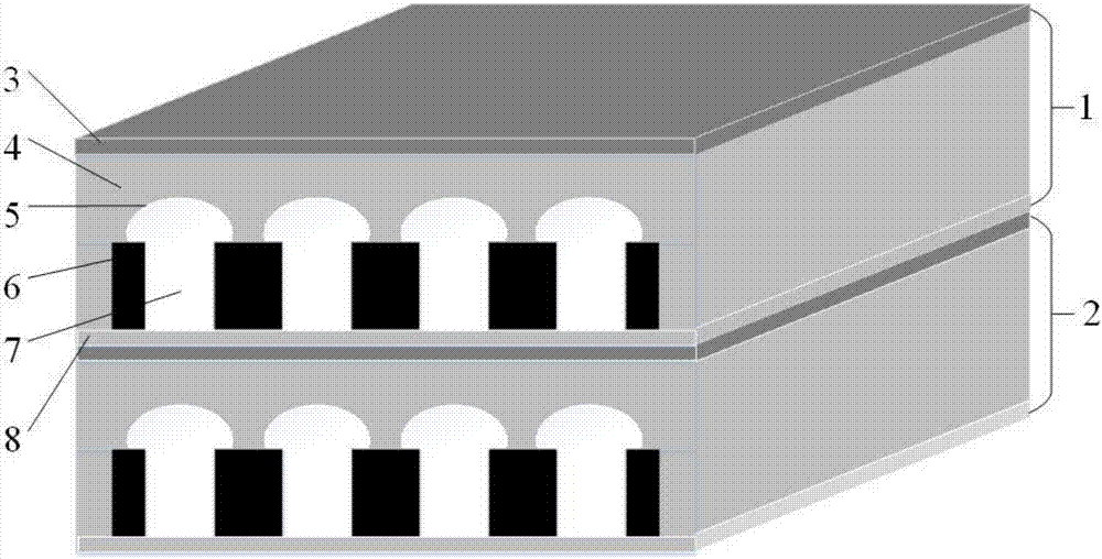
[0036] Embodiment 1, the silicon substrate sample thickness Hsi is 70 μm; the width Ws of the silicon carbide flow channel wall is 30 μm, the height Hc is 50 μm; the long diameter Wt of the silicon flow channel wall is 36 μm, and the height Ht is 20 μm for a three-dimensional integrated circuit Silicon carbide microfluidic cooling structure.

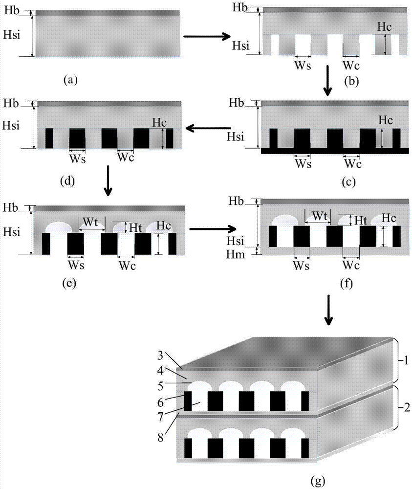
[0037] Step 1, grow the epitaxial layer, such as figure 2 (a).

[0038] An epitaxial layer with a thickness Hb of 2 μm is epitaxially grown on the front surface of a silicon substrate sample with a thickness Hsi of 70 μm for making a chip circuit.

[0039] Step 2, etch the silicon-based rectangular channel, such as figure 2 (b).

[0040] (2.1) Carry out chemical mechanical polishing, photoresist coating, drying, exposure and development photolithography to the back of the sample that has grown the epitaxial layer in sequence to form a photoresist mask;

[0041] (2.2) After the photoresist mask is formed, the silicon on the back of ...

Embodiment 2

[0055] Embodiment 2, the silicon substrate sample thickness Hsi is 150 μm; the width Ws of the silicon carbide flow channel wall is 100 μm, the height Hc is 120 μm; the long diameter Wt of the silicon flow channel wall is 130 μm, and the height Ht is a three-dimensional integrated circuit of 35 μm Silicon carbide microfluidic cooling structure.

[0056] Step 1, growing an epitaxial layer, that is, epitaxially growing an epitaxial layer with a thickness Hb of 6 μm on the front surface of a silicon substrate sample with a thickness Hsi of 150 μm, for making a chip circuit, such as figure 2 (a).

[0057] Step 2, etching the silicon-based rectangular channel, such as figure 2 (b).

[0058] (2a) Carrying out chemical mechanical polishing, photoresist coating, drying, exposure and development photolithography in sequence on the back of the sample that has grown the epitaxial layer to form a photoresist mask;

[0059] (2b) After the photoresist mask is formed, the silicon on the...

Embodiment 3

[0072] Embodiment 3, the silicon substrate sample thickness Hsi is 250 μm; the width Ws of the silicon carbide flow channel wall is 200 μm, the height Hc is 200 μm; the long diameter Wt of the silicon flow channel wall is 280 μm, and the height Ht is 200 μm for a three-dimensional integrated circuit Silicon carbide microfluidic cooling structure.

[0073] Step A, growing an epitaxial layer, that is, epitaxially growing an epitaxial layer with a thickness Hb of 10 μm on the front surface of a silicon substrate sample with a thickness Hsi of 250 μm, for making a chip circuit, such as figure 2 (a).

[0074] Step B, etching the silicon-based rectangular channel, such as figure 2 (b).

[0075] (B1) sequentially perform chemical mechanical polishing on the back of the sample that has completed the growth of the epitaxial layer;

[0076] (B2) Apply photoresist to the polished sample, dry, expose and develop photolithography, and form a photoresist mask on the sample;

[0077] (...


PUM

PropertyMeasurementUnit
thicknessaaaaaaaaaa
widthaaaaaaaaaa
heightaaaaaaaaaa

Abstract

The invention relates to a silicon carbide micro-channel heat dissipation structure of a three-dimensional integrated circuit and a manufacturing method thereof, and mainly solves the problem that a micro-channel wall material is low in heat conductivity and small in contact area with the micro-channel wall in the prior art. The silicon carbide micro-channel heat dissipation structure comprises an upper chip (1) and a lower chip (2), wherein each chip comprises a circuit layer (3), a silicon substrate (4), a silicon channel wall (5), a silicon carbide channel wall (6), a micro-channel (7) and a silicon micro-channel cap (8) from top to bottom, wherein each circuit layer is positioned on the top of the front side of the corresponding chip, and each silicon substrate is adjacent to the corresponding circuit layer and is positioned below the corresponding circuit layer; each silicon channel wall is adjacent to the corresponding silicon substrate and is positioned below the corresponding silicon substrate; each silicon carbide channel wall epitaxially grows below the corresponding silicon channel wall; the cross section of each micro-channel is of an integral structure with a semi-elliptical upper part and a rectangular lower part, and each micro-channel is positioned below the corresponding silicon channel wall. The heat dissipation contact area close to the circuit layers is increased, the distances with the circuit layers are shortened, and the heat dissipation performance of the micro-channel heat dissipation structure is improved.

Description

technical field [0001] The invention belongs to the technical field of microelectronics, and in particular relates to a silicon carbide microfluidic cooling structure, which can be used for cooling three-dimensional integrated circuits. technical background [0002] In the past few decades, the size of microelectronic devices has been continuously reduced according to Moore's law, and the performance of electronic products has been continuously improved. The integration density is getting higher and higher, and the number of transistors integrated on the chip has doubled; with the multi-functionalization and miniaturization of electronic products, the power consumption per unit chip has increased rapidly, the heat flow per unit volume has increased, and the chip temperature Improve rapidly. Due to the impact of temperature on the chip, the life of the chip is reduced; the temperature in different regions is different, and the excessively high temperature may also cause defo...

Claims


Application Information

Patent Timeline
Patent Type & Authority Applications(China)
IPC IPC(8): H01L23/473H01L23/373H01L25/065H01L21/98
CPCH01L23/473H01L23/373H01L25/0657H01L25/50
Inventor 董刚李秀慧杨银堂
Owner XIDIAN UNIV
Why Eureka
Try Eureka