Silicon carbide microfluidic heat dissipation structure of three-dimensional integrated circuit and manufacturing method thereof
A technology of integrated circuit and heat dissipation structure, applied in the field of microelectronics, can solve the problems affecting the electrical performance of the chip, small contact area, low thermal conductivity of silicon, etc., to achieve enhanced auxiliary heat dissipation capability, high thermal conductivity, and improved electrical performance Effect
- Summary
- Abstract
- Description
- Claims
- Application Information
AI Technical Summary
Problems solved by technology
Method used
Image
Examples
Embodiment 1
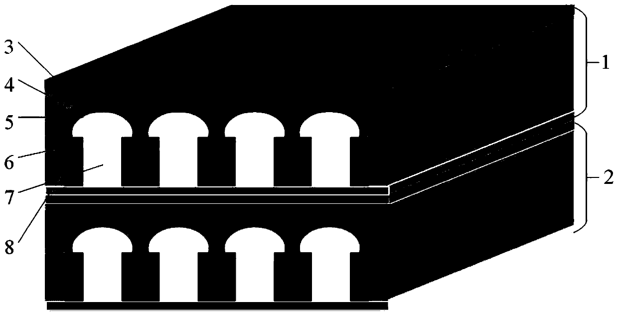
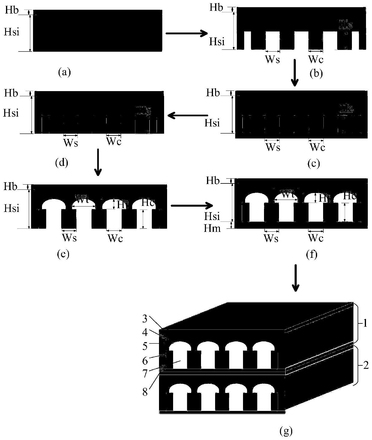
[0037] Embodiment 1, the silicon substrate sample thickness Hsi is 70 μm; the width Ws of the silicon carbide flow channel wall is 30 μm, the height Hc is 50 μm; the long diameter Wt of the silicon flow channel wall is 36 μm, and the height Ht is 20 μm for a three-dimensional integrated circuit Silicon carbide microfluidic cooling structure.
[0038] Step 1, grow the epitaxial layer, such as figure 2 (a).
[0039] An epitaxial layer with a thickness Hb of 2 μm is epitaxially grown on the front surface of a silicon substrate sample with a thickness Hsi of 70 μm for making a chip circuit.
[0040] Step 2, etch the silicon-based rectangular channel, such as figure 2 (b).
[0041] (2.1) Carry out chemical mechanical polishing, photoresist coating, drying, exposure and development photolithography to the back of the sample that has grown the epitaxial layer in sequence to form a photoresist mask;
[0042] (2.2) After the photoresist mask is formed, the silicon on the back of ...
Embodiment 2
[0056] Embodiment 2, the silicon substrate sample thickness Hsi is 150 μm; the width Ws of the silicon carbide flow channel wall is 100 μm, the height Hc is 120 μm; the long diameter Wt of the silicon flow channel wall is 130 μm, and the height Ht is a three-dimensional integrated circuit of 35 μm Silicon carbide microfluidic cooling structure.
[0057] Step 1, growing an epitaxial layer, that is, epitaxially growing an epitaxial layer with a thickness Hb of 6 μm on the front surface of a silicon substrate sample with a thickness Hsi of 150 μm, for making a chip circuit, such as figure 2 (a).
[0058] Step 2, etching the silicon-based rectangular channel, such as figure 2 (b).
[0059] (2a) Carrying out chemical mechanical polishing, photoresist coating, drying, exposure and development photolithography in sequence on the back of the sample that has grown the epitaxial layer to form a photoresist mask;
[0060] (2b) After the photoresist mask is formed, the silicon on the...
Embodiment 3
[0073] Embodiment 3, the silicon substrate sample thickness Hsi is 250 μm; the width Ws of the silicon carbide flow channel wall is 200 μm, the height Hc is 200 μm; the long diameter Wt of the silicon flow channel wall is 280 μm, and the height Ht is 200 μm for a three-dimensional integrated circuit Silicon carbide microfluidic cooling structure.
[0074] Step A, growing an epitaxial layer, that is, epitaxially growing an epitaxial layer with a thickness Hb of 10 μm on the front surface of a silicon substrate sample with a thickness Hsi of 250 μm, for making a chip circuit, such as figure 2 (a).
[0075] Step B, etching the silicon-based rectangular channel, such as figure 2 (b).
[0076] (B1) sequentially perform chemical mechanical polishing on the back of the sample that has completed the growth of the epitaxial layer;
[0077] (B2) Apply photoresist to the polished sample, dry, expose and develop photolithography, and form a photoresist mask on the sample;
[0078] (...
PUM
| Property | Measurement | Unit |
|---|---|---|
| thickness | aaaaa | aaaaa |
| width | aaaaa | aaaaa |
| height | aaaaa | aaaaa |
Abstract
Description
Claims
Application Information

