
GeSn material-based LED

A technology of crystallization and substrate, applied to LED. field, can solve the problems of poor performance of PINGeSn light-emitting tubes, unsatisfactory quality of GeSn layer materials, and high dislocation density of Ge epitaxial layer, so as to achieve the effects of suppressing the expansion of defects, improving luminous efficiency, and improving performance

Active Publication Date: 2017-10-13
道县晶维电子有限公司
View PDF3 Cites 0 Cited by
  • Summary
  • Abstract
  • Description
  • Claims
  • Application Information

AI Technical Summary

Problems solved by technology

The Ge epitaxial layer prepared by this method has high dislocation density and large surface roughness, and the quality of the GeSn layer material grown on it is not ideal, resulting in poor performance of the PINGeSn light-emitting tube.

Method used


Image

  • GeSn material-based LED
  • GeSn material-based LED
  • GeSn material-based LED

Examples


Embodiment 1

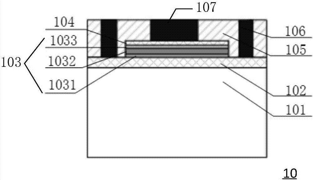
[0025] Please refer to figure 1 , figure 1 A structural schematic diagram of an LED (10) based on a GeSn material provided for an embodiment of the present invention, the LED (10) based on a GeSn material includes:

[0026] A substrate (101), a P-type crystallized Ge layer (102), an intrinsic Ge layer (103), an N-type Ge layer (104) and a passivation layer (105);

[0027] Wherein, the P-type crystallized Ge layer (102), the intrinsic Ge layer (103), the N-type Ge layer (104) and the passivation layer (105) are sequentially stacked on the substrate ( 101) on.

[0028] Further, on the basis of the foregoing embodiments, a positive electrode (106) and a negative electrode (107) are also included, and the positive electrode (106) and the negative electrode (107) are respectively connected to the P-type crystallized Ge layer (102) and said N-type Ge layer (104).

[0029] Further, on the basis of the above embodiments, both the positive electrode (106) and the negative electrode...

Embodiment 2

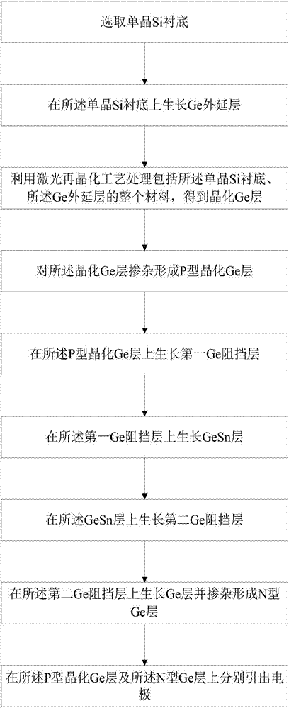
[0038] See figure 2 , figure 2 A flowchart of a method for manufacturing a GeSn-based LED based on an LRC process is provided in an embodiment of the present invention, wherein the LRC process refers to a laser recrystallization process. Specifically, the preparation method includes:

[0039] (a) select a single crystal Si substrate;

[0040] (b) growing a Ge epitaxial layer on the single crystal Si substrate;

[0041] (c) processing the entire material including the single crystal Si substrate and the Ge epitaxial layer by a laser recrystallization process to obtain a crystallized Ge layer;

[0042] (d) doping the crystallized Ge layer to form a p-type crystallized Ge layer;

[0043] (e) growing a first Ge barrier layer on the p-type crystallized Ge layer;

[0044] (f) growing a GeSn layer on the first Ge barrier layer;

[0045] (g) growing a second Ge barrier layer on the GeSn layer;

[0046] (h) growing a Ge layer on the second Ge barrier layer and doping to form a...

Embodiment 3

[0083] Please refer to Figure 3a-Figure 3m , Figure 3a-Figure 3m It is a schematic diagram of a method for preparing a vertical PIN GeSn light-emitting tube with a double intrinsic Ge barrier layer based on an LRC process according to an embodiment of the present invention, and the method includes the following steps:

[0084] S101, select single crystal Si substrate 001, such as Figure 3a shown.

[0085] S102. At a temperature of 250° C. to 350° C., a Ge seed layer 002 of 40 to 50 nm is grown on a single crystal Si substrate 001 by using a CVD process, such as Figure 3b shown.

[0086] S103, at a temperature of 550° C. to 600° C., using a CVD process to grow a Ge main layer 003 with a thickness of 150 to 250 nm on the surface of the Ge seed layer 002, such as Figure 3c shown.

[0087] S104, growing SiO with a thickness of 100-150 nm on the surface of the Ge main body layer 003 by using a CVD process 2 protective layer 004, such as Figure 3d shown.

[0088] S105,...


PUM

PropertyMeasurementUnit
Thicknessaaaaaaaaaa
Doping concentrationaaaaaaaaaa
Thicknessaaaaaaaaaa

Abstract

The invention relates to a GeSn material-based LED. The LED comprises a monocrystal Si substrate, a P type crystallization Ge layer, an intrinsic Ge layer and a SiO<2> passivation layer, wherein the monocrystal Si substrate, the P type crystallization Ge layer, the intrinsic Ge layer and the SiO<2> passivation layer are arranged in a stacked manner in sequence. According to the GeSn material-based LED provided by the embodiment, GeSn is adopted to replace Ge to be used as the light source in a photoelectric integrated circuit, so that luminous efficiency is improved and defect expansion can be suppressed effectively so as to obtain the high-quality Ge / Si virtual substrate; and in addition, a Ge barrier layer structure is introduced between the Ge doping layer and the GeSn intrinsic layer, so that unintentional doping to the GeSn by the doping source of the Ge layer can be avoided, thereby improving the performance of the device.

Description

technical field [0001] The invention belongs to the technical field of integrated circuits, in particular to an LED based on GeSn material. Background technique [0002] The development of integrated circuit technology, the increase of wafer size and the reduction of chip feature size can more easily meet the requirements of miniaturization, high density, high speed, high reliability and system integration. One of the longest used basic materials in integrated circuit technology is Si material. The Si substrate is used as the substrate to make the light source, which is easy to integrate and can reduce the cost. [0003] In recent years, Ge material is expected to become a light source in Si-based optoelectronic integrated circuits due to its integrability with Si and its unique energy band structure. The direct band gap of the Ge material is only 136meV higher than the indirect band gap, and the direct band luminescence wavelength (1550nm) of Ge is located in the C band. ...

Claims


Application Information

Patent Timeline
IPC IPC(8): H01L33/00H01L33/34H01L21/02
CPCH01L21/02532H01L21/02535H01L21/02683H01L33/0054H01L33/343
Inventor 刘晶晶
Owner 道县晶维电子有限公司
Learn More