

leds based on gesn materials
A crystallization, substrate technology, used in LEDs. It can solve the problems of poor performance of PINGeSn light-emitting tube, unsatisfactory quality of GeSn layer material, high dislocation density of Ge epitaxial layer, and achieve the effect of inhibiting the expansion of defects, improving luminous efficiency and improving performance.
- Summary
- Abstract
- Description
- Claims
- Application Information
AI Technical Summary
Problems solved by technology
Method used
Image

Examples
Embodiment 1
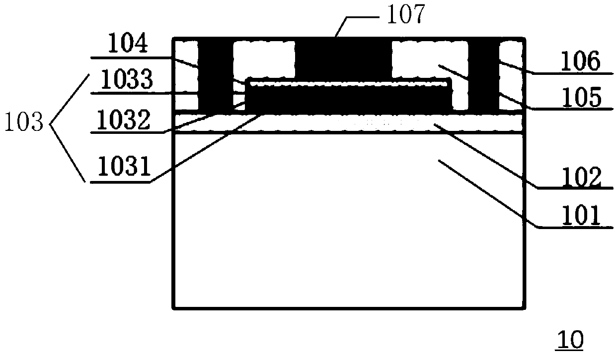
[0025] Please refer to figure 1 , figure 1 A structural schematic diagram of an LED (10) based on a GeSn material provided for an embodiment of the present invention, the LED (10) based on a GeSn material includes:
[0026] A substrate (101), a P-type crystallized Ge layer (102), an intrinsic Ge layer (103), an N-type Ge layer (104) and a passivation layer (105);
[0027] Wherein, the P-type crystallized Ge layer (102), the intrinsic Ge layer (103), the N-type Ge layer (104) and the passivation layer (105) are sequentially stacked on the substrate ( 101) on.
[0028] Further, on the basis of the foregoing embodiments, a positive electrode (106) and a negative electrode (107) are also included, and the positive electrode (106) and the negative electrode (107) are respectively connected to the P-type crystallized Ge layer (102) and said N-type Ge layer (104).
[0029] Further, on the basis of the above embodiments, both the positive electrode (106) and the negative electrode...
Embodiment 2
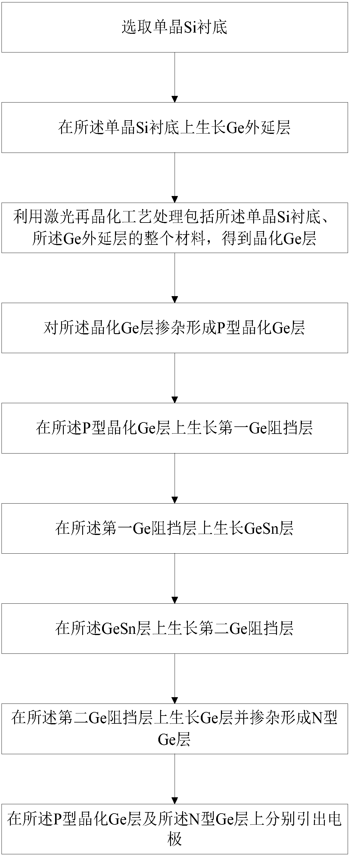
[0038] See figure 2 , figure 2 A flowchart of a method for manufacturing a GeSn-based LED based on an LRC process is provided in an embodiment of the present invention, wherein the LRC process refers to a laser recrystallization process. Specifically, the preparation method includes:
[0039] (a) select a single crystal Si substrate;
[0040] (b) growing a Ge epitaxial layer on the single crystal Si substrate;
[0041] (c) processing the entire material including the single crystal Si substrate and the Ge epitaxial layer by a laser recrystallization process to obtain a crystallized Ge layer;
[0042] (d) doping the crystallized Ge layer to form a p-type crystallized Ge layer;
[0043] (e) growing a first Ge barrier layer on the p-type crystallized Ge layer;
[0044] (f) growing a GeSn layer on the first Ge barrier layer;
[0045] (g) growing a second Ge barrier layer on the GeSn layer;
[0046] (h) growing a Ge layer on the second Ge barrier layer and doping to form a...
Embodiment 3
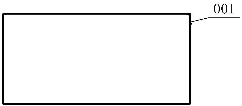
[0083] Please refer to Figure 3a-Figure 3m , Figure 3a-Figure 3m It is a schematic diagram of a method for preparing a vertical PIN GeSn light-emitting tube with a double intrinsic Ge barrier layer based on an LRC process according to an embodiment of the present invention, and the method includes the following steps:
[0084] S101, select single crystal Si substrate 001, such as Figure 3a shown.
[0085] S102. At a temperature of 250° C. to 350° C., a Ge seed layer 002 of 40 to 50 nm is grown on a single crystal Si substrate 001 by using a CVD process, such as Figure 3b shown.
[0086] S103, at a temperature of 550° C. to 600° C., using a CVD process to grow a Ge main layer 003 with a thickness of 150 to 250 nm on the surface of the Ge seed layer 002, such as Figure 3c shown.
[0087] S104, growing SiO with a thickness of 100-150 nm on the surface of the Ge main body layer 003 by using a CVD process 2 protective layer 004, such as Figure 3d shown.
[0088] S105,...
PUM
 Abstract
Description
Claims
Application Information