Packaging method of OLED panel

An encapsulation method and panel technology, which are applied in the manufacture of electrical components, electric solid-state devices, and semiconductor/solid-state devices, etc., can solve the problems of low film production rate, high price, and increased packaging cost of OLED panels, and achieve high equipment utilization, The effect of improving the packaging effect and reducing the packaging cost

Pending Publication Date: 2017-10-13
SHENZHEN CHINA STAR OPTOELECTRONICS SEMICON DISPLAY TECH CO LTD
View PDF7 Cites 13 Cited by
  • Summary
  • Abstract
  • Description
  • Claims
  • Application Information

AI Technical Summary

Problems solved by technology

The conventional method to solve the above problems is to form a protective layer or passivation layer (Passivation) on the cathode by chemical vapor deposition (chemical vapor deposition, CVD) or atomic layer deposition (Atomic Layer Deposition, ALD). It is a silicon nitride (SiN) layer or a silicon oxide (SiO) layer, etc. However, CVD equipment and ALD equipment are expensive, and the film production rate is low, resulting in an increase in the packaging cost of the OLED panel
[0006] In the past two years, the exploration of flexible OLED panel packaging has been in full swing. However, the packaging cost of flexible OLED devices will increase by 1-5 times the cost of traditional cover plate packaging. Although flexible OLED display is the future display trend, the traditional Cover-encapsulated OLED panels are not going away

Method used


Image

  • Packaging method of OLED panel
  • Packaging method of OLED panel
  • Packaging method of OLED panel

Examples


no. 1 example

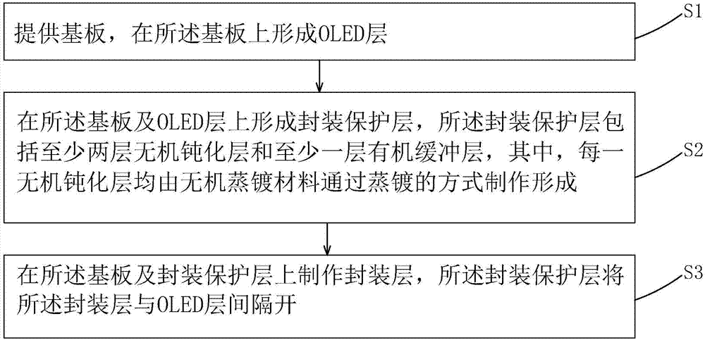
[0032] see figure 1 , the present invention provides a method for encapsulating an OLED panel. The first embodiment of the method for encapsulating an OLED panel of the present invention specifically includes the following steps:

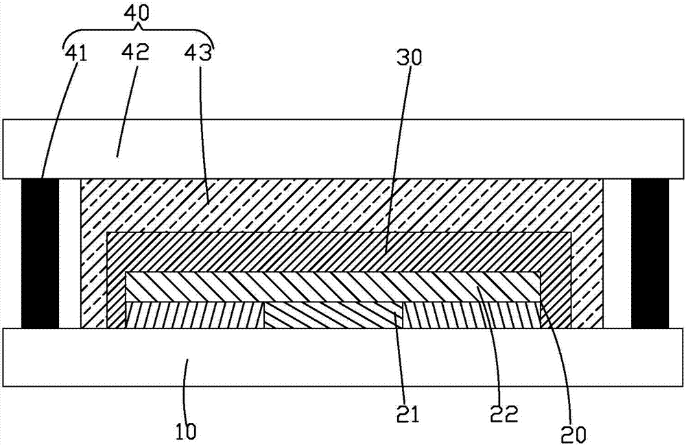
[0033] Step S1 , providing a substrate 10 on which an OLED layer 20 is formed.

[0034] Specifically, the substrate 10 is a thin film transistor (TFT) array substrate with a TFT layer 11 thereon, and the base substrate of the substrate 10 can be a rigid substrate, such as a glass substrate, or a flexible substrate, such as a flexible Polyimide (PI) substrate.

[0035] Specifically, the OLED layer 20 formed in the step S1 includes an anode layer (not shown), an organic functional layer 21 and a cathode layer 22 sequentially arranged from bottom to top.

[0036] Specifically, the OLED panel can be a top-emission OLED panel, and the cathode layer 22 is formed by vapor deposition, and its material is magnesium-silver alloy (Mg / Ag), or it can be a bott...


PUM


Abstract

The invention provides a packaging method of an OLED panel. As a packaging protection layer and an inorganic passivation layer are formed on a base plate and an OLED layer by adopting an evaporation way, the packaging layer and the OLED layer can be separated efficiently, a minute amount of moisture or solvents in the packaging layer further can be prevented from permeating to the interior of the OLED device to result in dark spots of a luminous zone, and the packaging effect of the OLED panel is further improved; in addition, for a top transmission type OLED panel, packaging Mura also can be prevented. Meanwhile, as the inorganic passivation layer is formed by adopting the evaporation way, the packaging cost of the OLED panel can be reduced efficiently; the inorganic passivation layer can be formed through direct evaporation after the OLED layer is formed through evaporation; the packaging method is convenient to operate; and the equipment utilization rate is high.

Description

technical field [0001] The invention relates to the field of flat panel display technology, in particular to a packaging method for an OLED panel. Background technique [0002] Organic light emitting diode (Organic Light Emitting Display, OLED) display device has self-illumination, low driving voltage, high luminous efficiency, short response time, high definition and contrast, nearly 180° viewing angle, wide operating temperature range, and can realize flexible display and With many advantages such as large-area full-color display, it is recognized by the industry as a display device with the most potential for development. [0003] OLED devices generally include: a substrate, an anode disposed on the substrate, a hole injection layer disposed on the anode, a hole transport layer disposed on the hole injection layer, a light emitting layer disposed on the hole transport layer, a An electron transport layer on the light emitting layer, an electron injection layer on the ele...

Claims


Application Information

Patent Timeline
Patent Type & Authority Applications(China)
IPC IPC(8): H01L51/52H01L51/56
CPCH10K50/841H10K50/84H10K50/846H10K50/844H10K71/00
Inventor 李文杰李金川
Owner SHENZHEN CHINA STAR OPTOELECTRONICS SEMICON DISPLAY TECH CO LTD
Why Eureka
Try Eureka