
Method for etching SiC through metal/oxide double-layer mask structure

A technology of oxide mask and metal mask, applied in semiconductor/solid-state device manufacturing, electrical components, circuits, etc., can solve problems such as metal elements contaminating SiC, and achieve the effect of reducing interface defects, increasing costs, and smoothing the surface

Inactive Publication Date: 2017-10-20
SHANGHAI INST OF MICROSYSTEM & INFORMATION TECH CHINESE ACAD OF SCI
View PDF4 Cites 10 Cited by
  • Summary
  • Abstract
  • Description
  • Claims
  • Application Information

AI Technical Summary

Problems solved by technology

[0004] In view of the shortcomings of the prior art described above, the purpose of the present invention is to provide a method for etching SiC using a metal / oxide double-layer mask structure, which is used to solve the problem of using a single layer of metal as a mask in the prior art. The problem of metallic elements contaminating SiC

Method used


Image

  • Method for etching SiC through metal/oxide double-layer mask structure
  • Method for etching SiC through metal/oxide double-layer mask structure
  • Method for etching SiC through metal/oxide double-layer mask structure

Examples


Embodiment Construction

[0041] Embodiments of the present invention are described below through specific examples, and those skilled in the art can easily understand other advantages and effects of the present invention from the content disclosed in this specification. The present invention can also be implemented or applied through other different specific implementation modes, and various modifications or changes can be made to the details in this specification based on different viewpoints and applications without departing from the spirit of the present invention.

[0042] Please refer to attached picture. It should be noted that the diagrams provided in this embodiment are only schematically illustrating the basic idea of ​​the present invention, and only the components related to the present invention are shown in the diagrams rather than the number, shape and shape of the components in actual implementation. Dimensional drawing, the type, quantity and proportion of each component can be change...


PUM

PropertyMeasurementUnit
thicknessaaaaaaaaaa

Abstract

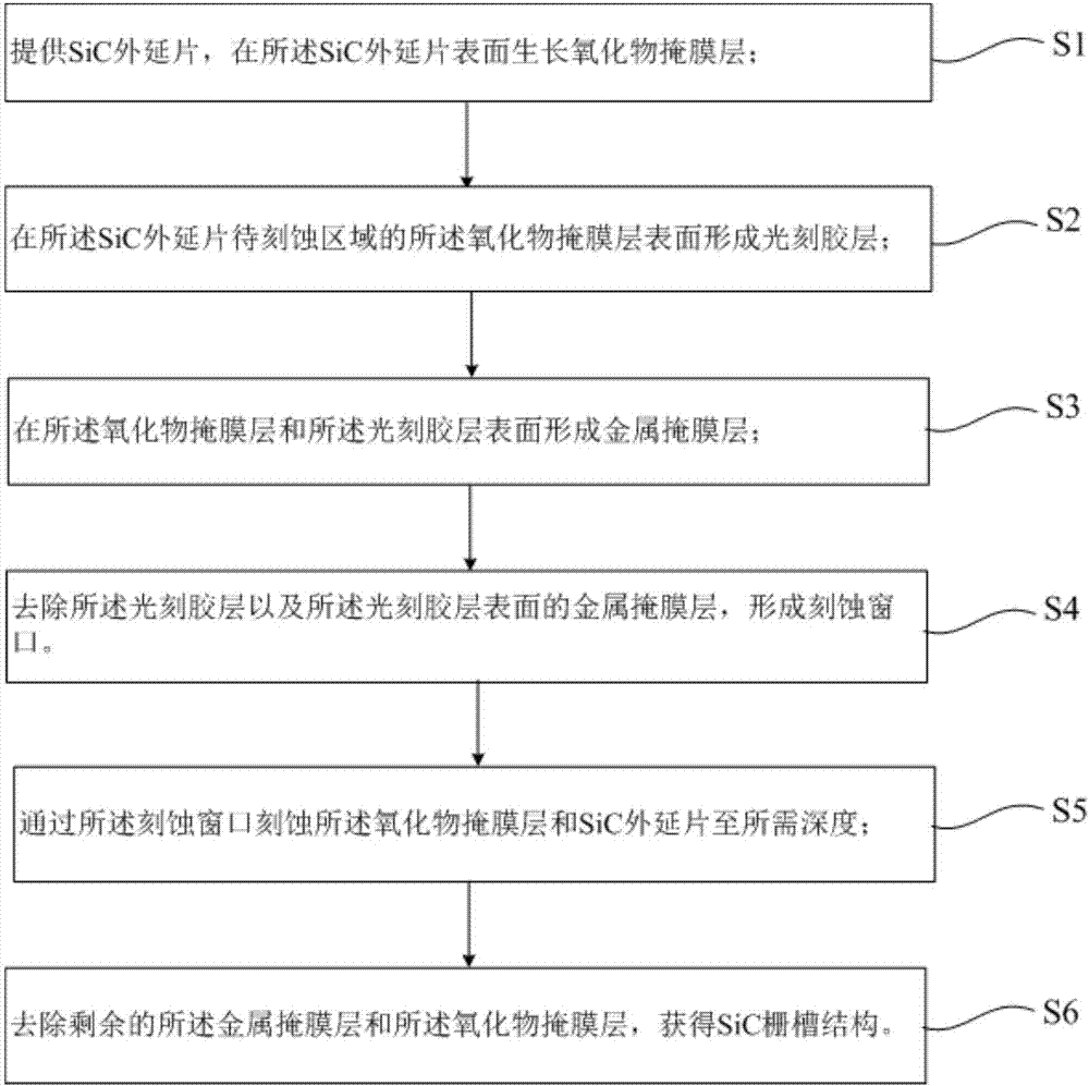
The invention provides a method for etching SiC through a metal / oxide double-layer mask structure, and the method at least comprises the steps: 1), providing an SiC epitaxial wafer, and growing an oxide mask layer on the surface of the SiC epitaxial wafer; 2), forming a photoresist layer on the surface of the oxide mask layer of a to-be-etched region of the SiC epitaxial wafer; 3), forming metal mask layers on the oxide mask layer and the surface of the photoresist layer; 4), removing the photoresist layer and the metal mask layer on the surface of the photoresist layer, and forming an etching window; 5), etching the oxide mask layer and the SiC epitaxial wafer to a needed depth through the etching window; 6), removing the residual metal mask layer and oxide mask layer, and obtaining an SiC gate groove structure. According to the invention, the oxide mask layer is taken as a blocking layer, thereby preventing the metal elements from diffusing towards the SiC epitaxial wafer and the substrate, and solving a problem of element pollution. In addition, the method can obtain a high-etching-rate gate and high-anisotropism groove structure with the smooth etching surface.

Description

technical field [0001] The invention relates to the field of semiconductor device manufacturing, in particular to a method for etching SiC by using a metal / oxide double-layer mask structure. Background technique [0002] Silicon carbide (SiC) material, as the third-generation wide bandgap semiconductor material, has the characteristics of high critical breakdown electric field, high thermal conductivity, and high electron saturation drift rate. It has great application potential in harsh environments such as high temperature or strong corrosiveness. [0003] For SiC gate trench structure devices such as UMOSFET, Trench Gate IGBT and SiC MEMS devices with three-dimensional structure, etch morphology, etch damage and etch surface residues have a great impact on the development and performance of SiC devices. The main difficulty in etching silicon carbide lies in the high mechanical hardness and chemical stability of silicon carbide materials. The actual process proves that t...

Claims


Application Information

Patent Timeline
Patent Type & Authority Applications(China)
IPC IPC(8): H01L21/033
CPCH01L21/0332
Inventor 程新红王谦李静杰郑理沈玲燕张栋梁顾子悦钱茹俞跃辉
Owner SHANGHAI INST OF MICROSYSTEM & INFORMATION TECH CHINESE ACAD OF SCI
Learn More