Constant-transconductance rail-to-rail operational amplifier

An operational amplifier, full swing technology, used in amplifiers, differential amplifiers, amplifiers with semiconductor devices/discharge tubes, etc., can solve the problems of difficult frequency compensation, non-constant transconductance, etc., to achieve constant equivalent transconductance, The effect of improving common mode rejection ratio and good stability

CN107301308AActive Publication Date: 2017-10-27SUZHOU KAIWEITE SEMICON
3 Cites 16 Cited by

Patent Information

Authority / Receiving Office
CN · China
Patent Type
Applications(China)
Current Assignee / Owner
Publication Date
2017-10-27

Smart Images

  • Figure 1
    Figure 1
  • Figure 2
    Figure 2
  • Figure 3
    Figure 3
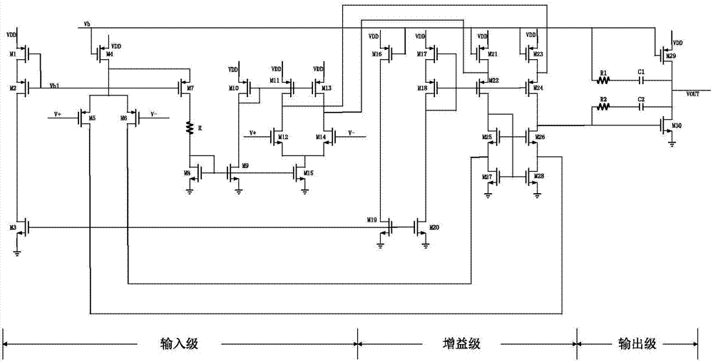
Patent Text Reader

Abstract

The invention relates to a constant-transconductance rail-to-rail operational amplifier. The constant-transconductance rail-to-rail operational amplifier comprises a rail-to-rail input stage, a gain stage and an output stage in sequential connection. The rail-to-rail input stage a PMOS (p-channel metal oxide semiconductor) differential pair, an NMOS (n-channel metal oxide semiconductor) differential pair, PMOS differential pair and NMOS differential pair tail current sources and an NMOS differential pair load circuit, and the PMOS differential pair and the NMOS differential pair are complementary. The gain stage comprises a self-bias cascade current mirror, and source electrodes of NMOS tubes and PMOS tubes of the PMOS differential pair and the NMOS differential pair are connected with the self-bias cascade current mirror. The output stage comprises a first PMOS tube, a first NMOS tube and a Miller compensator, the first PMOS tube and the first NMOS tube are in common-source connection, grid electrodes of the first PMOS tube and the first NMOS tube are connected with the self-bias cascade current mirror, and the Miller compensator is formed by series connection of a Miller compensation capacitor and a compensation resistor. The constant-transconductance rail-to-rail operational amplifier has advantages that input stage constant transconductance in a full voltage operating range can be guaranteed effectively, the whole circuit structure is high in stability, the operating voltage range of the operational amplifier is expanded, low-voltage application is realized, and the common-mode rejection ratio of the operational amplifier is increased.
Need to check novelty before this filing date? Find Prior Art

Description

technical field

[0001] The invention relates to the field of integrated circuit design, in particular to an operational amplifier, in particular to a rail-to-rail folded cascode across-conductor full-swing operational amplifier. Background technique

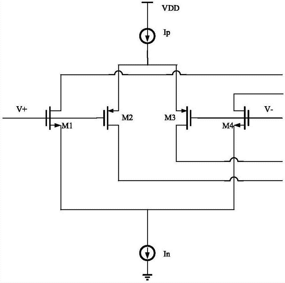
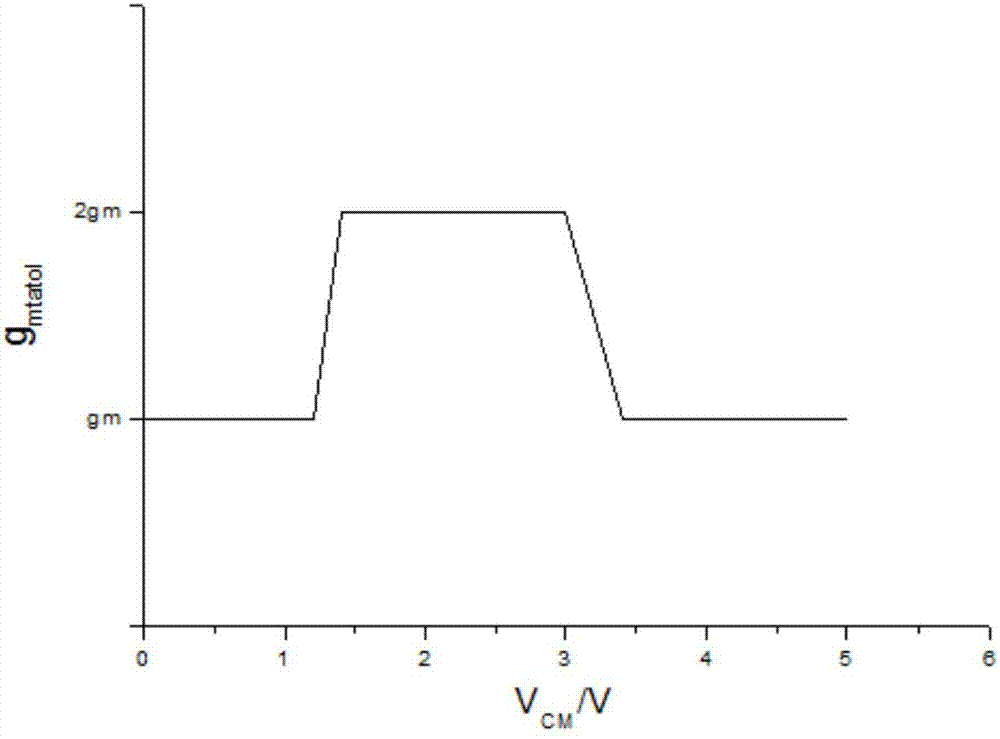
[0002] A traditional rail-to-rail operational amplifier uses complementary PMOS and NMOS differential pairs as the input stage, and its structure is as follows figure 1 As shown, among them, M2 and M3 are PMOS differential input pairs, and M1 and M4 are NMOS differential input pairs. In this way, in the lower input voltage range, the PMOS differential input pair works, and the NMOS differential pair turns off; in the higher input voltage range, the NMOS differential input pair works, and the PMOS differential pair turns off; only in the middle input voltage In the range, the NMOS and PMOS differential pairs work at the same time. Thus, the total common-mode input range is the full swing V SS <V CM <V DD .

[0003] H...

Examples

Embodiment Construction

[0018] In order to deepen the understanding and recognition of the present invention, the present invention will be further described and introduced below in conjunction with the accompanying drawings.

[0019] Such as image 3 and 4 As shown, a constant transconductance full-swing operational amplifier includes a rail-to-rail input stage, a gain stage, and an output stage connected in sequence. The rail-to-rail input stage includes complementary PMOS differential pairs and NMOS differential pairs, PMOS The tail current source of the differential pair and the NMOS differential pair, and the load circuit of the NMOS differential pair. The PMOS differential pair is realized by two PMOS transistors M5 and M6 connected to the common source, wherein the gate of the PMOS transistor M5 is drawn out as an operational amplifier. The non-inverting input terminal, the gate of the PMOS transistor M6 is used as the inverting input terminal of the operational amplifier, and the NMOS differen...