Preparation method of metal atom-doped large-area regular epitaxial graphene

A technology of metal atoms and graphene, applied in graphene, semiconductor/solid-state device manufacturing, electrical components, etc., can solve problems affecting electrical characteristics and destroying the flatness of graphene sheets, so as to achieve controllable doping types and ideas Effects of clear and simplified growth and doping processes

Active Publication Date: 2017-11-03
XI AN JIAOTONG UNIV
View PDF6 Cites 5 Cited by
  • Summary
  • Abstract
  • Description
  • Claims
  • Application Information

AI Technical Summary

Problems solved by technology

The non-equilibrium pyrolysis process of conventional vacuum annealing tends to produce a large number of micropores and atomic steps on the surface of graphene, which seriously damages the flatness of graphene sheets and affects its electrical properties.

Method used


Image

  • Preparation method of metal atom-doped large-area regular epitaxial graphene
  • Preparation method of metal atom-doped large-area regular epitaxial graphene
  • Preparation method of metal atom-doped large-area regular epitaxial graphene

Examples


Embodiment 1

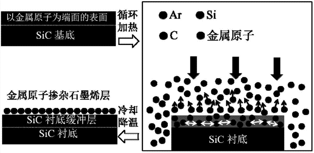
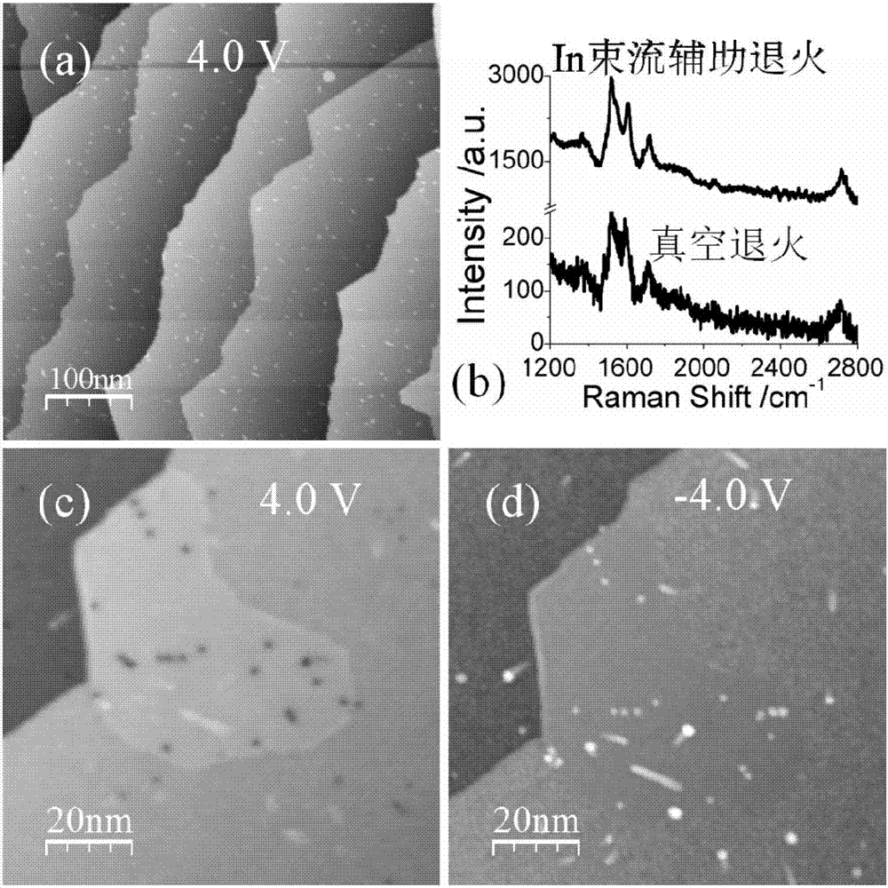
[0034] The single crystal 6H-SiC(0001) sample was heated to about 540°C for 8 hours under 0.5A direct current; using the K-Cell device, the metal In source was heated to 700°C, the heating current was 2.8A, and the In atoms The beam size was controlled at 26nA; at the same time, the SiC sample was heated to 1100°C with a current of 1.1A, and heated and annealed under the In beam for 10min, and the surface temperature of the sample was monitored and controlled by an infrared thermometer; after cooling to room temperature, the Ar The atmosphere was passed into the sample preparation chamber and the vacuum was maintained at 5 × 10 -5 Torr; use a current of 1.8A to raise the temperature of the sample to 1450°C and heat and anneal for 5 minutes, then reheat after cooling for 2 minutes, and repeat this cycle 5 times; in this example, a large-area regular epitaxial graphene doped with metal In atoms was obtained, and its scanning Tunneling microscope morphology and Raman test results...

Embodiment 2

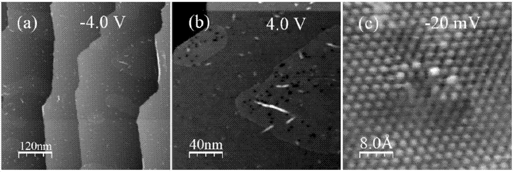
[0036]The single crystal 6H-SiC(0001) sample was heated to 550°C for 8 hours under the direct current condition of 0.51A; using the K-Cell device, the metal Ag source was heated to 730°C, the heating current was 3.0A, and the Ag atom beam The current size is controlled at 30nA; at the same time, the SiC sample is heated to 1100°C with a current of 1.15A, heated and annealed for 10 minutes, and the surface temperature of the sample is monitored and controlled by an infrared thermometer; after the annealing is completed and cooled to room temperature, the Ar atmosphere is introduced into the sample preparation chamber, and maintain a vacuum of 5 x 10 -5 Torr; use a current of 1.9A to heat the sample to 1450°C for 5 minutes, heat it after cooling for 2 minutes, and recycle 4 times; this example prepares a large-area regular epitaxial graphene doped with metal Ag atoms, and its scanning tunnel Microscopic morphology and atomic resolution images such as image 3 shown.

Embodiment 3

[0038] The single crystal 6H-SiC(0001) sample was heated to 530°C for 8h under DC condition of 0.48A; using the K-Cell device, the metal Bi source was heated to 710°C, the heating current was 2.6A, and the Bi atomic beam The current size is controlled at 24nA; at the same time, the SiC sample is heated to 1130°C with a current of 1.2A and heated and annealed for 10min, and the surface temperature of the sample is monitored and controlled by an infrared thermometer; after cooling to room temperature, the Ar atmosphere is introduced into the sample preparation chamber, and maintain a vacuum of 5 x 10 - 5 Torr; use a current of 1.8A to raise the temperature of the sample to 1450°C and heat and anneal for 5 minutes, then cool for 2 minutes and then reheat, and so cycle 4 times; this example obtained a large-area regular epitaxial graphene doped with metal Bi atoms, which Scanning tunneling microscope morphology and atomic resolution images such as Figure 4 shown.


PUM

PropertyMeasurementUnit
thicknessaaaaaaaaaa

Abstract

The invention discloses a preparation method of metal atom-doped large-area regular epitaxial graphene, and applied to the technical field of microelectronics. Metal atoms are introduced to a SiC pyrolysis process and Ar atmosphere is adopted for protection in an auxiliary manner, so that the large-area regular epitaxial graphene can be prepared, external metal atoms also can be guided to be directly participated in a graphene lamination layer growth process, thereby promoting atom intercalation or hybridization between metal atoms and C atoms to realize doping of metal atoms, and avoiding damage to the overall structure of graphene caused by ion implantation; pretreatment of metal atom beams is the important premise of realizing doping, and by virtue of the Ar atmosphere environment, generate of surface holes can be suppressed, so that regular and uniform surface appearance of the epitaxial graphene sample is ensured; and the preparation method is simple in technical idea, high in operability, is a stable and effective metal atom doping method, and capable of providing significant guidance and reference to optimization preparation and performance improvement of epitaxial graphene.

Description

technical field [0001] The invention belongs to the technical field of preparation and modification of two-dimensional thin film materials, and relates to a preparation method of large-area regular epitaxial graphene doped with metal atoms. Background technique [0002] Epitaxial graphene is produced by high-temperature pyrolysis of single-crystal SiC substrates. It can be directly applied to the production of electronic devices without transfer. It is expected to become an ideal candidate semiconductor material in the silicon-based post-Moore era. IBM Corporation of the United States has developed a field-effect transistor based on epitaxial graphene with a frequency up to 300 GHz, which has given people high hopes for its application in the field of microelectronics technology. Recently, more and more researchers are working on the large-area preparation, metal doping and regulation of the physical properties of epitaxial graphene. The interaction between metal atoms and ...

Claims


Application Information

Patent Timeline
Patent Type & Authority Applications(China)
IPC IPC(8): H01L21/02C01B32/188
CPCC01P2002/82H01L21/02378H01L21/02527H01L21/0257
Inventor 胡廷伟马飞徐可为马大衍刘祥泰张晓荷
Owner XI AN JIAOTONG UNIV
Why Eureka
Try Eureka