

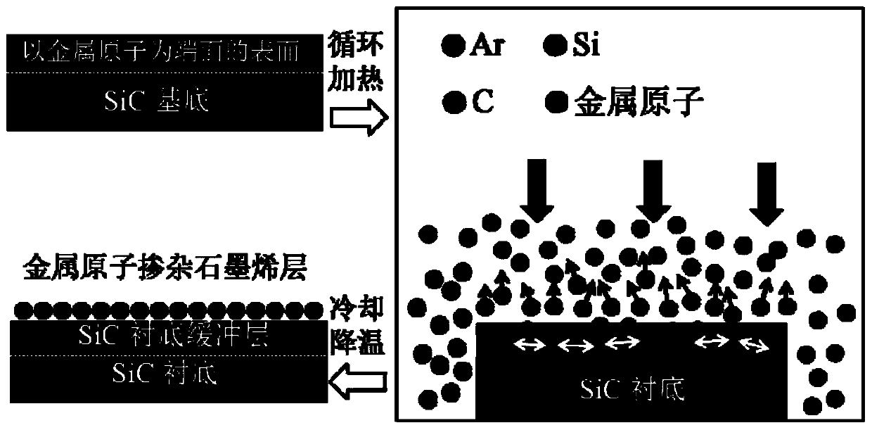
A method for preparing large-area regular epitaxial graphene doped with metal atoms
A technology of metal atoms and graphene, which is applied in the direction of graphene, semiconductor/solid-state device manufacturing, nano-carbon, etc., can solve the problems of destroying the flatness of graphene sheets and affecting electrical properties, etc. Control and destroy small effects
- Summary
- Abstract
- Description
- Claims
- Application Information
AI Technical Summary
Problems solved by technology
Method used
Image

Examples
Embodiment 1
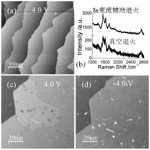
[0034] The single crystal 6H-SiC(0001) sample was heated to about 540°C under 0.5A direct current to degas for 8 hours; using the K-Cell device, the metal In source was heated to 700°C, the heating current was 2.8A, and the In atoms The beam size was controlled at 26nA; at the same time, the SiC sample was heated to 1100°C with a current of 1.1A, and heated and annealed under the In beam for 10min, and the surface temperature of the sample was monitored and controlled by an infrared thermometer; after cooling to room temperature, the Ar The atmosphere was passed into the sample preparation chamber and the vacuum was maintained at 5 × 10 -5 Torr; use a current of 1.8A to raise the temperature of the sample to 1450°C and heat and anneal for 5 minutes, then reheat after cooling for 2 minutes, and repeat this cycle 5 times; in this example, a large-area regular epitaxial graphene doped with metal In atoms was obtained. Tunneling microscope morphology and Raman test results are as ...
Embodiment 2
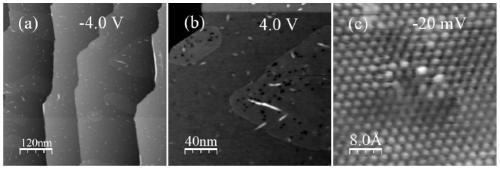
[0036] The single crystal 6H-SiC(0001) sample was heated to 550°C for 8 hours under the condition of direct current of 0.51A; using the K-Cell device, the metal Ag source was heated to 730°C, the heating current was 3.0A, and the Ag atom beam The current size is controlled at 30nA; at the same time, the SiC sample is heated to 1100°C with a current of 1.15A, heated and annealed for 10 minutes, and the surface temperature of the sample is monitored and controlled by an infrared thermometer; after the annealing is completed and cooled to room temperature, the Ar atmosphere is introduced into the sample preparation chamber, and maintain a vacuum of 5 x 10 -5Torr; use a current of 1.9A to heat the sample to 1450°C for 5 minutes, heat it after cooling for 2 minutes, and recycle 4 times; this example prepares a large-area regular epitaxial graphene doped with metal Ag atoms, and its scanning tunnel Microscopic morphology and atomic resolution images such as image 3 shown.
Embodiment 3
[0038] The single crystal 6H-SiC(0001) sample was heated to 530°C for 8h under DC condition of 0.48A; using the K-Cell device, the metal Bi source was heated to 710°C, the heating current was 2.6A, and the Bi atomic beam The current size is controlled at 24nA; at the same time, the SiC sample is heated to 1130°C with a current of 1.2A and heated and annealed for 10 minutes, and the surface temperature of the sample is monitored and controlled by an infrared thermometer; after cooling to room temperature, the Ar atmosphere is introduced into the sample preparation chamber, and maintain a vacuum of 5 x 10 -5 Torr; with a current of 1.8A, the sample was heated to 1450°C and heated and annealed for 5 minutes, then cooled for 2 minutes and then heated again, and this cycle was repeated 4 times; in this example, a large-area regular epitaxial graphene doped with metal Bi atoms was obtained. Scanning tunneling microscope morphology and atomic resolution images such as Figure 4 show...
PUM
| Property | Measurement | Unit |
|---|---|---|
| thickness | aaaaa | aaaaa |
Abstract
Description
Claims
Application Information