Preparation method of perovskite thin film with light control structure and optical device

A technology of perovskite and light regulation, applied in semiconductor/solid-state device manufacturing, electric solid-state devices, semiconductor devices, etc., can solve the problems of poor controllability, high cost, high pressure, etc., and achieve improved optoelectronic performance, low cost, Simple preparation process

Active Publication Date: 2019-12-13
SUZHOU UNIV
View PDF8 Cites 0 Cited by
  • Summary
  • Abstract
  • Description
  • Claims
  • Application Information

AI Technical Summary

Problems solved by technology

This method is usually used to introduce the structure of soft material thin films, but for perovskite crystal thin films, a very large pressure is required, and the template needs a material with high hardness, which is costly and poorly controllable.

Method used


Image

  • Preparation method of perovskite thin film with light control structure and optical device
  • Preparation method of perovskite thin film with light control structure and optical device
  • Preparation method of perovskite thin film with light control structure and optical device

Examples


Embodiment 1

[0045] Embodiment 1 has the preparation method of the perovskite film of photoregulatory structure

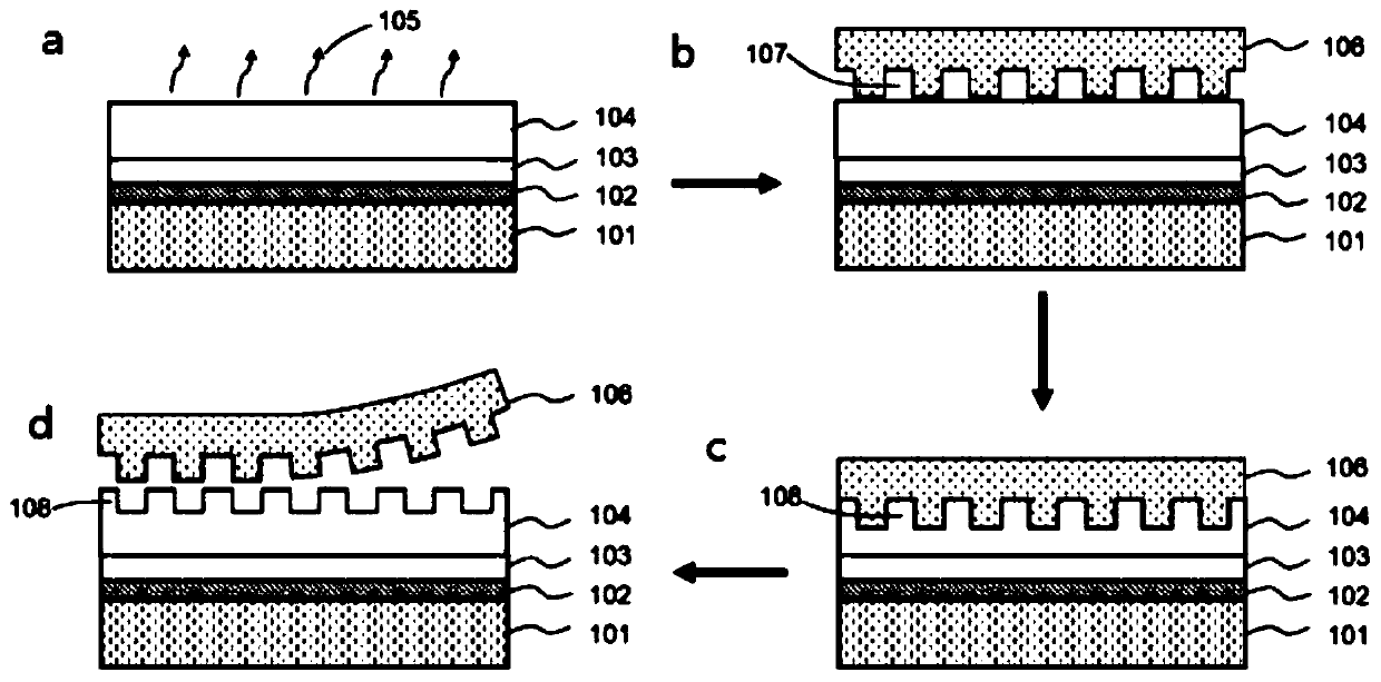
[0046] Such as figure 1 As shown, the preparation method of the perovskite film with light-tuning structure is as follows:

[0047] After the substrate substrate 101 made of glass is cleaned with detergent, a patterned ITO thin film is sputtered on one side as the transparent electrode layer 102 . Place the substrate substrate with ITO in detergent, deionized water, acetone, ethanol, and deionized water in sequence, and ultrasonically clean it for 10 minutes each time. After cleaning, dry it with a nitrogen gun, and put the substrate substrate into the ultraviolet UV ozone treatment was carried out in an ozone machine for 10 min.

[0048] The above-mentioned substrate substrate was transferred to a glove box, and a layer of PEDOT:PSS was spin-coated on the surface of the substrate as the hole transport layer 103, and the rotation speed was controlled to 4000rpm, and the time ...

Embodiment 2

[0053] The preparation method of embodiment 2 solar cells

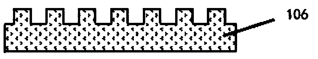
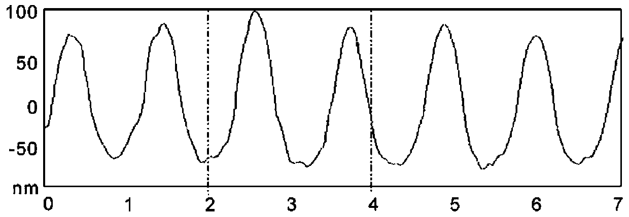
[0054] When preparing the battery, the shape of the nano concave-convex structure used is a one-dimensional periodic grating structure, the groove depth is 150nm, the period is 800nm, and the duty ratio is 0.6.

[0055] The specific manufacturing process of each layer structure of the transparent electrode layer 102, the hole transport layer 103, the perovskite film 104, the electron transport layer 15, the buffer layer 16 and the metal electrode 17 on the substrate substrate 101 can be selected from the solution method respectively. Methods such as spin coating, vapor deposition, sputtering, or other known methods, preferably, in this embodiment, the specific steps are as follows:

[0056] (1) Ordinary float glass substrate After the substrate 101 is cleaned with detergent, a patterned ITO film is sputtered on one side as the transparent electrode layer 102 . Place the substrate substrate with ITO in detergent, deio...

Embodiment 3

[0063] The preparation method of embodiment 3 light-emitting diodes

[0064] When preparing the light-emitting diode, the shape of the nano concave-convex structure used is a one-dimensional periodic grating structure, the groove depth is 150nm, the period is 400nm, and the duty ratio is 0.6.

[0065] The specific method is as follows:

[0066] (1) Ordinary float glass substrate After the substrate 101 is cleaned with detergent, a patterned ITO film is sputtered on one side as the transparent electrode layer 102 . Place the substrate substrate with ITO in detergent, deionized water, acetone, ethanol, and deionized water in sequence, and ultrasonically clean it for 10 minutes each time. After cleaning, dry it with a nitrogen gun, and put the substrate substrate into the ultraviolet Carry out ultraviolet ozone treatment in the ozone machine for 10 minutes;

[0067] (2) Transfer the substrate substrate processed in step (1) to a glove box, spin-coat a layer of PEDOT:PSS on the ...


PUM

PropertyMeasurementUnit
thicknessaaaaaaaaaa
thicknessaaaaaaaaaa
thicknessaaaaaaaaaa

Abstract

The invention relates to a method for preparing a perovskite thin film with a light-regulating structure: providing a substrate and a template with a nano-concave-convex structure, the template is a soft material; coating a perovskite precursor solution on the surface of the substrate, and vacuum treatment 10-30min, to volatilize part of the solvent to obtain the treated substrate; cover the template on the treated substrate, and then carry out co-annealing and crystallization under the pressure of 5-10bar, remove the template, and obtain the perovskite grown on the surface of the substrate film. The present invention also provides a method for preparing a photoelectric device. Using the method for preparing a perovskite film, the substrate is pre-coated with a conductive electrode layer and a first transmission layer, and the surface of the perovskite film is modified sequentially from bottom to top The second transmission layer, the buffer layer and the metal electrode, wherein the structures among the perovskite film, the second transmission layer, the buffer layer and the metal electrode are complementary. The invention utilizes the micro-nano template to control the directional growth of the perovskite, and directly introduces light-regulating nanostructures into the perovskite thin film.

Description

technical field [0001] The invention relates to the technical field of optoelectronic devices, in particular to a perovskite film with a light-regulating structure and a preparation method of an optical device. Background technique [0002] Perovskite materials refer to those with ABX 3 A class of materials with a structure in which A and B represent cations and X represents anions. This kind of material has the advantages of fast carrier diffusion speed, long diffusion distance, direct band gap, suitable band gap, high light absorption, electron and hole transmission, simple preparation, low cost, and good comprehensive performance. In recent years, solar cells based on perovskite materials have developed rapidly, and their certified efficiency has reached 22.1%, which has exceeded the efficiency of dye-sensitized solar cells and organic solar cells that have been developed for decades, and even gradually approached crystalline silicon solar cells. At the same time, perov...

Claims


Application Information

Patent Timeline
Patent Type & Authority Patents(China)
IPC IPC(8): H01L51/05H01L51/42H01L51/44H01L51/30H01L51/46B82Y30/00
CPCB82Y30/00H10K71/12H10K85/30H10K10/20H10K30/00H10K30/87Y02E10/549Y02P70/50
Inventor 唐建新许瑞鹏魏健李艳青
Owner SUZHOU UNIV
Why Eureka
Try Eureka