

Dry film developing solution for printed circuit board and preparation method of dry film developing solution
A technology for printed circuit boards and developer, which is applied in the chemical industry, can solve the problems of large developer waste water treatment, easy generation of a large number of bubbles, and increased production costs, so as to reduce residual image phenomenon, reduce decomposition rate and corrosiveness, The effect of promoting clearance
- Summary
- Abstract
- Description
- Claims
- Application Information
AI Technical Summary
Problems solved by technology
Method used
Image

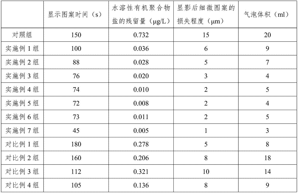
Examples
Embodiment 1
[0030] Embodiment 1, a kind of dry film developer for printed circuit board
[0031] The dry film developer for printed circuit boards is composed of the following components and content:
[0032] Potassium carbonate 0.2kg, sodium carbonate 0.8kg, sodium hypochlorite 0.08kg and water 95kg.
[0033] Preparation:
[0034] S1 Add potassium carbonate and sodium carbonate to water, stir until completely dissolved to obtain a mixed solution;
[0035] S2 Add sodium hypochlorite to the mixed solution obtained in step S1 and stir evenly to obtain final product.
Embodiment 2
[0036] Embodiment 2, a kind of dry film developing solution for printed circuit board
[0037] The dry film developer for printed circuit boards is composed of the following components and content:
[0038] Potassium carbonate 0.4kg, sodium carbonate 0.5kg, sodium hypochlorite 0.1kg and water 99kg.
[0039] The preparation method is similar to Example 1.
Embodiment 3
[0040] Embodiment 3, a kind of dry film developer for printed circuit board
[0041] The dry film developer for printed circuit boards is composed of the following components and content:
[0042] Potassium carbonate 0.4kg, sodium carbonate 0.5kg, sodium hypochlorite 0.1kg, sodium alginate 4kg and water 99kg.
[0043] Preparation:
[0044] S1 Add potassium carbonate and sodium carbonate to water, stir until completely dissolved to obtain a mixed solution;
[0045] S2 Add sodium hypochlorite and sodium alginate to the mixed solution obtained in step S1 and stir evenly to obtain.
PUM
 Abstract
Description
Claims
Application Information