Parallel light micro-spot optical key dimension analysis device and detection method

A technology of key dimensions and detection methods, applied in the field of optical engineering, can solve the problems of RCWA calculation efficiency and other problems, and achieve the effect of overcoming the long time consumption

Inactive Publication Date: 2017-11-14
FUJIAN INST OF RES ON THE STRUCTURE OF MATTER CHINESE ACAD OF SCI
View PDF5 Cites 3 Cited by
  • Summary
  • Abstract
  • Description
  • Claims
  • Application Information

AI Technical Summary

Problems solved by technology

Although RCWA is very suitable for diffraction simulation of vertical sidewall periodic structures, complex periodic structures with arbitrary shapes often need to be calculated by step approximation techniques
It is worth noting that the multi-layer division of the ladder approximation has a great impact on the computational efficiency of RCWA, because for the multi-layer model, RCWA needs to calculate the eigenvalues ​​layer by layer, which is a time-consuming problem.

Method used


Image

  • Parallel light micro-spot optical key dimension analysis device and detection method
  • Parallel light micro-spot optical key dimension analysis device and detection method
  • Parallel light micro-spot optical key dimension analysis device and detection method

Examples


Embodiment 1

[0061] In order to more intuitively reflect the characteristics of the detection method of the optical critical dimension test / analysis system of the present invention, the embodiment selects the simulation efficiency of complex two-dimensional periodic structures to illustrate the difference between the RCWA / SAM detection method and the traditional RCWA detection and analysis tool .

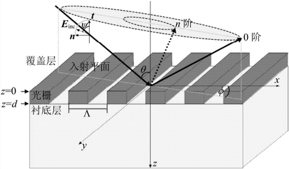
[0062] The surface structure of the sample is as Figure 5 As shown, the simplified shallow trench isolation (STI) 3D structure (left picture) and the simplified physical model (right picture) have a period of 402.9nm and 122.8nm in the x and y directions. The structure is a core-shaped elliptical array with non-vertical side walls. The major axis of the upper base in the x direction is 176.2 nm, the minor axis in the y direction is 30 nm, the major axis of the lower base in the x direction is 220 nm, and the minor axis in the y direction is 65 nm. The materials of the grating layer are all Si,...

Embodiment 2

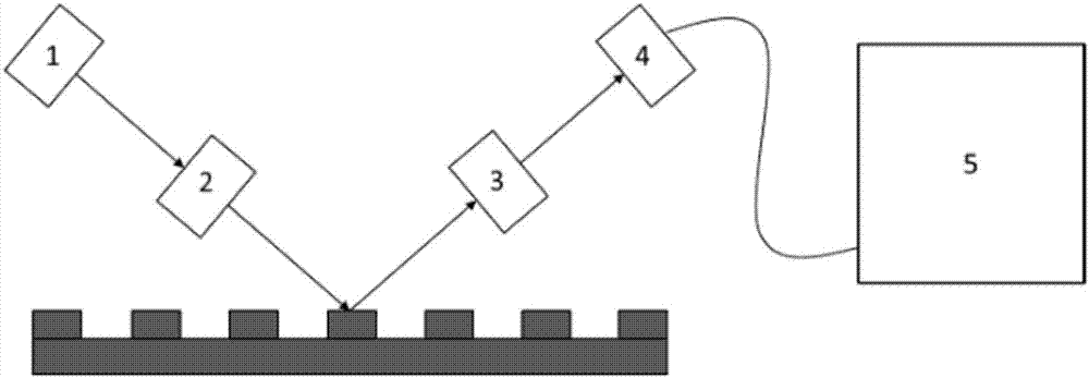
[0066] The detection of the sample and the zero-order diffraction curve of the sample is the same as in Embodiment 1, wherein the detection lens 3 is connected to the spectrometer 4 through an optical fiber.

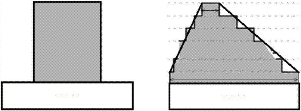
[0067] Curve simulation and comparison methods are different, specifically, Figure 5 The structure shown is a two-dimensional periodic structure, which is divided into 500 steps and approximate thin layers for simulation. The single simulation time for the test / analysis of critical dimensions is relatively long. Therefore, a mathematical and physical model database based on the structural parameters of the critical dimensions of the sample is established first. Example built in 10 4 Quantitative mathematical physical model, and calculate the simulated zero-order diffraction curve database of the sample mathematical physical model. The simulated zero-order diffraction curve database is compared with the measured zero-order diffraction curve of the sample by traversal me...

Embodiment 3

[0069] The device and detection method are the same as in Example 1, and the parameter curve of concern is replaced by an elliptical polarization parameter curve from the zero-order diffraction curve, and 100 step-approximate thin layers are divided for simulation. The analysis results are basically the same as in Example 1, and the time spent is reduced by 50%. .


PUM


Abstract

The present invention discloses a parallel light micro-spot optical key dimension detection method. With the detection method adopted, a vertical sidewall structure and a non-vertical sidewall structure in a microelectronic structure can be analyzed. According to the detection method, a parameter-of-interest curve of a sample is detected through a spectrograph; a microelectronic periodic structure physical model of key dimension information such as the grating period, duty ratio and grating thickness of the structure of the sample is built to perform simulation calculation, so that the zero-order diffraction rate curve of the sample can be obtained; fitting analysis is performed on the zero-order diffraction rate curve which is obtained through simulation and a zero-order diffraction rate curve detected by the spectrograph; and the key dimensions of the microelectronic periodic structure to be tested are obtained through inversion. The present invention discloses a detection device for the above method. The detection device can detect and analyze the vertical sidewall structure and non-vertical sidewall structure in the microelectronic structure and can detect and analyze the non-vertical sidewall structure quickly. The method and device can quickly detect and analyze the non-vertical sidewall structure.

Description

technical field [0001] The invention belongs to the field of optical engineering, and relates to a simulation detection method of a microelectronic structure optical critical dimension test / analysis system. Background technique [0002] In the semiconductor and other microelectronics industries, effective and rapid detection of the critical dimension (CD) of the microelectronic structure is an important means to improve the yield and efficiency of mass production of chips during the design and manufacture of chip structures. The chip has a high degree of integration. After a series of processes such as plate making, photolithography, and etching, the structure (Pattern) on the chip will form a periodic arrangement. There are many methods for measuring the size of periodically arranged microstructures, such as traditional optical microscopy, microscopy (EM), probe microscopy (SPM) and so on. However, these detection methods either require complex microscope equipment, or req...

Claims


Application Information

Patent Timeline
Patent Type & Authority Applications(China)
IPC IPC(8): G01B11/00
CPCG01B11/00
Inventor 陈树强邓浩朱振国余金清
Owner FUJIAN INST OF RES ON THE STRUCTURE OF MATTER CHINESE ACAD OF SCI
Why Eureka
Try Eureka