Semiconductor structure and manufacturing method thereof

A manufacturing method and semiconductor technology, applied in the fields of semiconductor/solid-state device manufacturing, semiconductor devices, electrical components, etc., can solve the problem that the electrical performance of semiconductor devices needs to be improved, and achieve the effect of avoiding adverse effects, optimizing electrical performance, and avoiding voids

Active Publication Date: 2017-11-14
SEMICON MFG INT (SHANGHAI) CORP +1
View PDF7 Cites 7 Cited by
  • Summary
  • Abstract
  • Description
  • Claims
  • Application Information

AI Technical Summary

Problems solved by technology

[0004] Although the introduction of high-k metal gates can improve the electrical performance of semiconductor devices to

Method used


Image

  • Semiconductor structure and manufacturing method thereof
  • Semiconductor structure and manufacturing method thereof
  • Semiconductor structure and manufacturing method thereof

Examples


Example Embodiment

[0014] It can be known from the background technology that the electrical performance of the semiconductor device formed by the prior art needs to be improved.

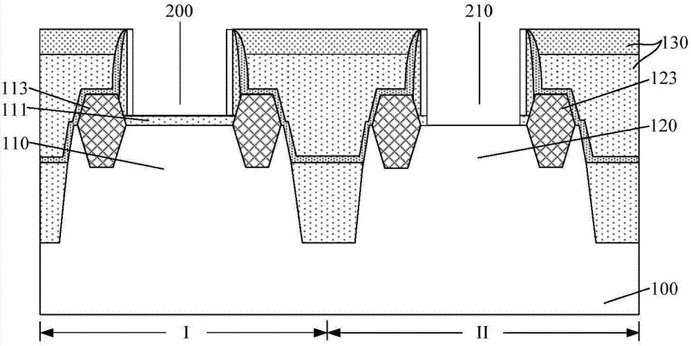
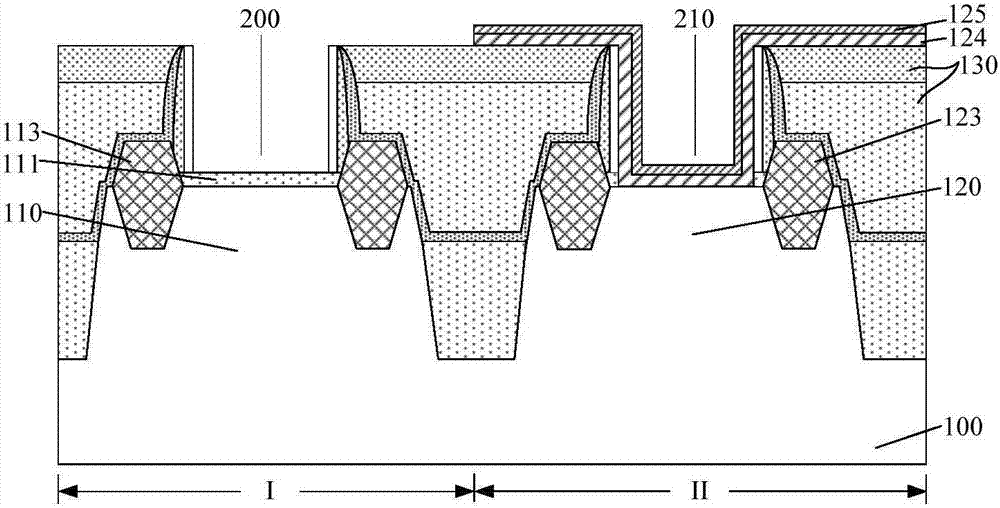
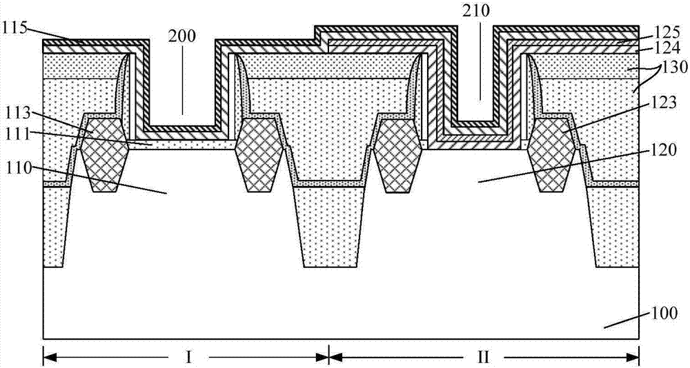
[0015] It has been found through research that in order to simultaneously meet the requirements of improving the threshold voltage (Threshold Voltage) of NMOS transistors and PMOS transistors in MOS transistors, different metal materials are usually used as the work function (WF, WorkFunction) in the metal gate structure of NMOS transistors and PMOS transistors. ) Layer material, so that the NMOS transistor and the PMOS transistor have different threshold voltages, wherein the metal gate structure of the NMOS transistor has an N-type work function layer, and the metal gate structure of the PMOS transistor has a P-type work function layer.

[0016] In this embodiment, the work function layer of the PMOS transistor is formed first and then the work function layer of the NMOS transistor is formed as an example for description....


PUM


Abstract

The invention provides a semiconductor structure and a manufacturing method thereof. The manufacturing method comprises the steps of: providing a substrate comprising a first region and a second region; forming an interlayer dielectric layer on the substrate; forming a first opening through which the substrate is exposed in the interlayer dielectric layer in the first region, and forming a second opening through which the substrate is exposed in the interlayer dielectric layer in the second region; forming gate dielectric layers on the bottom part and the side wall of the first opening as well as that of the second opening; forming a second work function layer on the gate dielectric layer in the second region; converting a partial thickness of the second work function layer into a barrier layer; forming a first work function layer on the gate dielectric layer in the first region and the barrier layer in the second region; and forming a metal layer which fills up the first opening and the second opening. According to the semiconductor structure and the manufacturing method thereof, the partial thickness of the second work function layer is converted into the barrier layer, the barrier layer can prevent metal ions in the first work function layer from diffusing into the second work function layer, and an additional film layer is not introduced, thereby avoiding adverse influence on the performance of the second work function layer.

Description

technical field [0001] The invention relates to the field of semiconductors, in particular to a semiconductor structure and a manufacturing method thereof. Background technique [0002] The main semiconductor device of an integrated circuit, especially a very large scale integrated circuit, is a metal-oxide-semiconductor field effect transistor (MOS transistor). With the continuous development of integrated circuit manufacturing technology, the technology nodes of semiconductor devices continue to decrease, and the geometric dimensions of semiconductor devices follow Moore's law. When the size of semiconductor devices is reduced to a certain extent, various secondary effects caused by the physical limits of semiconductor devices appear one after another, and it becomes more and more difficult to scale down the feature size of semiconductor devices. Among them, in the field of semiconductor manufacturing, the most challenging thing is how to solve the problem of large leakag...

Claims


Application Information

Patent Timeline
IPC IPC(8): H01L29/423H01L21/8238
CPCH01L21/8238H01L21/823842H01L21/823857H01L29/4232H01L29/42356H01L29/42364
Inventor 周飞
Owner SEMICON MFG INT (SHANGHAI) CORP
Why Eureka
Try Eureka