Non-substrate medium layer, and semiconductor device using same

A technology without substrates and semiconductors, applied in semiconductor devices, semiconductor/solid-state device parts, electric solid-state devices, etc., can solve the problems of difficult flip-chip bonding process, inability to perform high-temperature tempering, dissociation or process cracking, etc., to achieve Avoid damage and cracks, precise conductive channels, increase the effect of quantity and density

Inactive Publication Date: 2017-11-17
李志雄
View PDF9 Cites 2 Cited by
  • Summary
  • Abstract
  • Description
  • Claims
  • Application Information

AI Technical Summary

Problems solved by technology

But even so, if the thickness of the wafer substrate after grinding is too thin, it is still easy to crack in the subsequent dissociation or process
Moreover, since the viscose used can only withstand a temperature of about 200 degrees Celsius, it cannot be processed in a high-temperature furnace tube, nor can it be subjected to a high-temperature tempering process.
In addition, the wafer substrate and the carrier attached to each other are not integrally formed, and it is also prone to bursting in a high temperature environment, and it is also easy to cause difficulties in the subsequent flip-chip bonding process
[0009] It can be seen that the above-mentioned existing interposers using preformed substrates obviously have many inconveniences and defects, no matter in terms of manufacture, structure and use, so further improvement is required in structure
In view of this, the inventor of the present invention has conducted in-depth discussions on the structural problems of the existing interposer, and has successfully developed a Substrate-free interposers that do not use preformed substrates and their semiconductor devices can effectively solve the inconvenience and troubles caused by the need to use perforated substrates for existing ones

Method used


Image

  • Non-substrate medium layer, and semiconductor device using same
  • Non-substrate medium layer, and semiconductor device using same
  • Non-substrate medium layer, and semiconductor device using same

Examples


Embodiment Construction

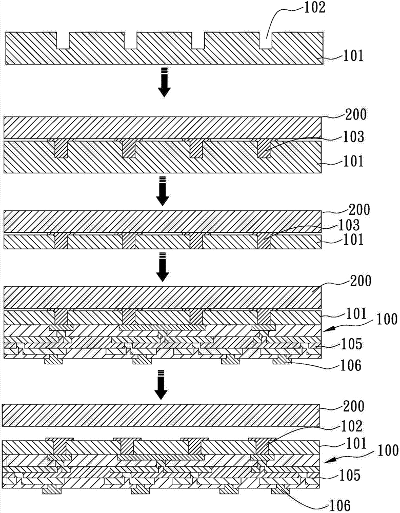
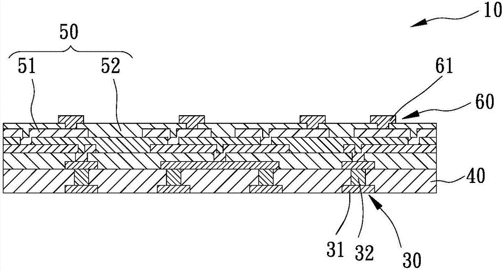
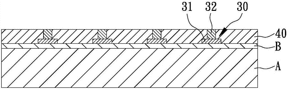
[0034] The present invention is a substrate-free interposer and a semiconductor device using it. The technical content of the present invention will be described below with reference to a specific embodiment, so that those familiar with the art can easily understand the advantages of the present invention from the content disclosed in this specification. and efficacy. However, the present invention can also be implemented or applied by virtue of other different specific implementation forms. Therefore, all references to front and rear, left and right, top and bottom, upper and lower, and horizontal and vertical in the specific embodiments of the present invention and their components in the accompanying drawings are only for convenience of description and are not limiting The invention, neither is intended to limit its components to any position or orientation in space. The dimensions specified in the drawings and description can be changed according to the design and require...


PUM


Abstract

The invention provides a non-substrate medium layer, and a semiconductor device using same, and especially, relates to a non-substrate medium layer which is free from using substrates, such as a prefabricated wafer, glass or organic layers. In the non-substrate medium layer, a plurality of conductive pathways, which connecting an upper and a lower surfaces, are formed in an insulation separation layer formed by deposition, coating and the like technologies in a solidifying manner. At least one wire rearrangement layer is arranged on one side surface of the insulation separation layer. The wire rearrangement layers are respectively provided with a dielectric layer and a plurality of wire patterns. In addition, a plurality of electrode pathways, which are electrically connected to a part of the wire patterns, are formed on the most-outer wire rearrangement layer on the insulation separation layer. By such way, thickness of the insulation separation layer is effectively controlled, and the conductive pathways are more accurate and micronized, numbers and density of pins thereon are greatly increased, and the medium layer is reduced in thickness and is more suitable for heating, compressing processes in later treatment. The non-substrate medium layer is effectively increased in production speed and qualification rate, and can satisfy demands in the following packaging processes.

Description

technical field [0001] The present invention relates to the field of interposer technology for semiconductor devices, and specifically refers to a substrate-free interposer structure that does not use preformed wafers, glass or organic layer substrates, so as to meet the requirements of thinning and The need for more signal pins reduces unnecessary processing sequences, and at the same time has the effect of improving the yield of semiconductor devices and reducing costs. Background technique [0002] By the way, with the vigorous development of the electronics industry, electronic products tend to be thinner and shorter in shape, so the semiconductor devices used in them are gradually stepping into the research and development direction of high performance, high function, and high speed. Semiconductor wafers on devices are being miniaturized continuously. Usually the most direct way to miniaturize semiconductor wafers is to rely on the refinement of lithography technology....

Claims


Application Information

Patent Timeline
Patent Type & Authority Applications(China)
IPC IPC(8): H01L23/31H01L23/528
CPCH01L23/31H01L23/3121H01L23/528
Inventor 李志雄
Owner 李志雄
Why Eureka
Try Eureka