Fabrication of conductive nanostructures on a flexible substrate

Inactive Publication Date: 2011-10-06
3M INNOVATIVE PROPERTIES CO
View PDF4 Cites 30 Cited by
  • Summary
  • Abstract
  • Description
  • Claims
  • Application Information

AI Technical Summary

Benefits of technology

[0006]There is a need for a continuous flexible nanostructured or microstructured sheet having a replicated base structure having at least a

Problems solved by technology

While molding technologies may be used in combination with the master replication tool to make a continuous roll of product, the resolution achiev

Method used


Image

  • Fabrication of conductive nanostructures on a flexible substrate
  • Fabrication of conductive nanostructures on a flexible substrate
  • Fabrication of conductive nanostructures on a flexible substrate

Examples


example 1

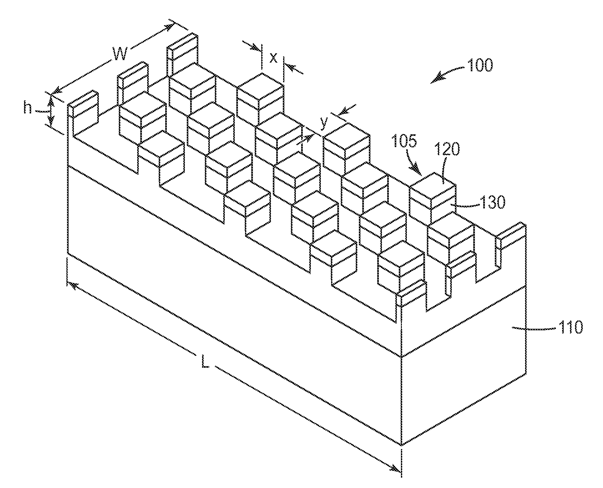
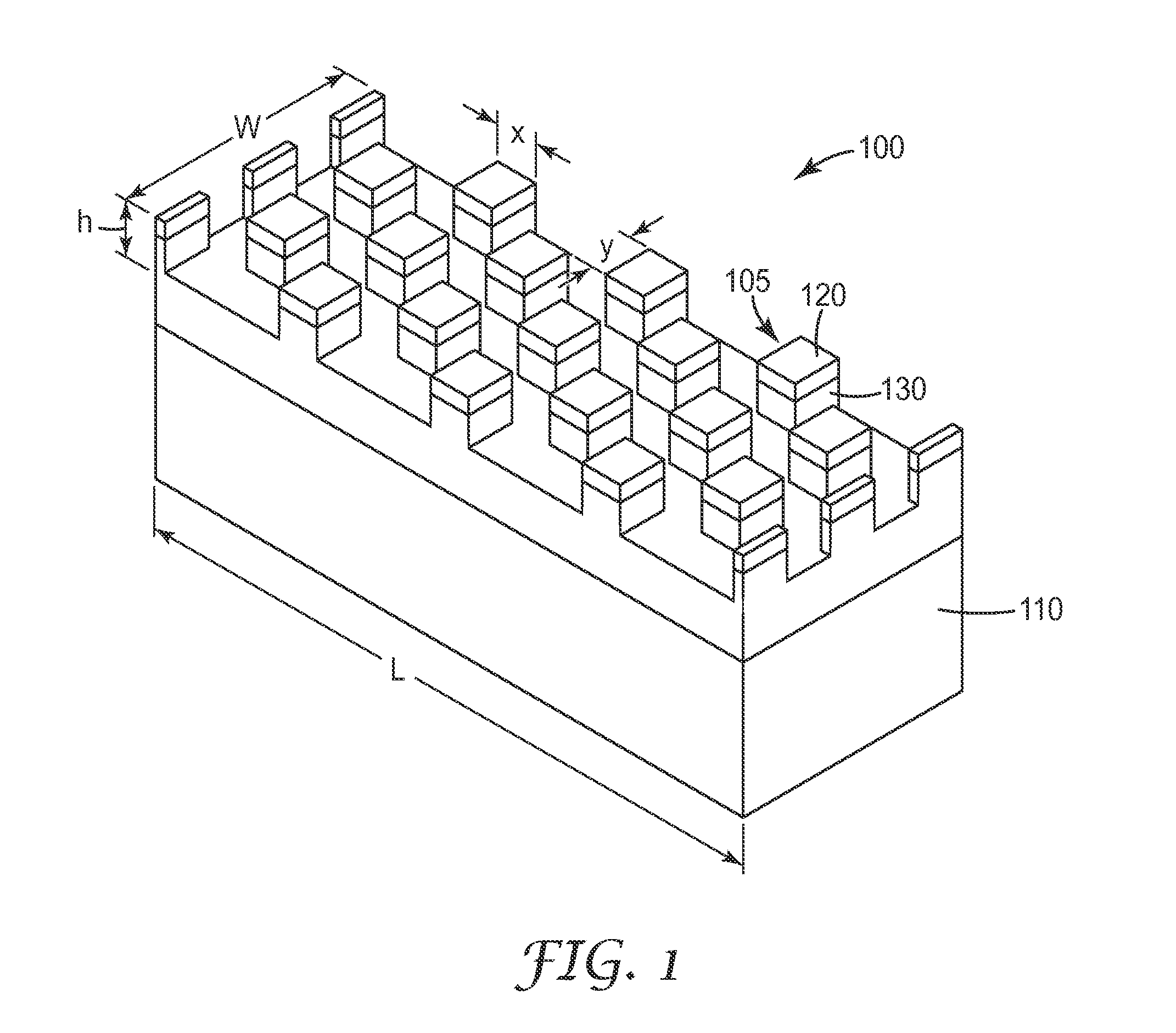
[0053]A nanostructured material 100′ having a sub-micron hole array structure was prepared utilizing the fabrication method previously described. FIGS. 3A-3G show a flow diagram of the fabrication method by which the nanostructured material 100′ was formed.

Preparing the Master

[0054]A thin layer of a positive UV5 photoresist 306 (available from Rohm and Haas Electronic Materials, Marlborough, Mass.) was applied to a glass master 300 having a conductive ITO surface layer 304 with a thin chromium tie layer (not shown) between the glass layer 302 and the ITO layer 304 as shown in FIG. 3A. The relief pattern 310 was made by interference lithography using a Innova Sabre FReD UV laser with an output of 270 mW (available from Company Coherent located at Santa Clara, Calif.) to pattern the photoresist layer 306 with an array of posts 314 (FIG. 3B). The exposed areas were then removed using a developing solution to dissolve the undesired photoresist.

[0055]The diameter, D, of the nanostructure...

example 2

[0061]A second replication master was made with a durable diamond-like carbon (DLC) relief structure on the surface of an ITO glass coated silicon master. A 200 nm DLC film was vacuum coated onto the surface of the ITO glass followed by application of a thin layer (about 50 nm) diamond-like glass (DLG) as described in U.S. Pat. Nos. 5,888,594; 6,015,597; and 6,696,157; herein incorporated by reference. A layer of photo resist (UV5 photoresist 306, available from Rohm and Haas Electronic Materials, Marlborough, Mass.) is applied to the to the DLG surface. The photo resist was patterned using interference lithography as generally described in U.S. Pat. No. 7,085,450, herein incorporated by reference. A 3-step reactive ion etching process utilizing perfluoropropane (C3F8), oxygen and argon gases was used to transfer the pattern from the photoresist into the DLC layer so that the surface of the ITO glass was exposed in selected areas. FIG. 5 shows a schematic cross-section of the silico...


PUM

PropertyMeasurementUnit
Currentaaaaaaaaaa
Electrical conductoraaaaaaaaaa
Thermoplasticityaaaaaaaaaa

Abstract

Provided is a method of fabricating a continuous nanostructured material having an electrodeposited surface layer. A conductive master drum having a relief pattern on its surface that exposes only a portion of the master drum surface is immersed into a plating bath. An electrodepositable material is coated onto the exposed surface of the drum. A support material is coated over the deposited layer and the relief structure. Removal from the drum yields the nanostructured material.

Description

FIELD OF THE INVENTION[0001]This application relates to a method for fabricating nanostructured and / or microstructured articles utilizing a continuous web-based process.BACKGROUND OF THE INVENTION[0002]Microstructured and nanostructured devices, for example, can be used in articles such as flat panel displays, chemical sensors, and bioabsorption substrates. Conventional methods for producing microstructured and nanostructured devices include molding a compliant material using a pressing or printing technology to reproduce a molded pattern, lithographic processes, and nanoimprint lithography.[0003]Articles with microstructured and nanostructured topographies include a plurality of structures on a surface thereof (projections, depressions, grooves and the like) that are microscopic in at least two dimensions or having at least one dimension that measures less than a micron in the cases of a nanostructured topography. These topographies may be created in or on the article by any contac...

Claims


Application Information

Patent Timeline
IPC IPC(8): C25D1/00
CPCB82Y20/00C25D5/02C25D1/006G02B5/3025G02B2207/101C25D5/028C25D1/003B82B1/00B82B3/00B82Y40/00
Inventor WANG, DINGPORQUE, JEROME C.
Owner 3M INNOVATIVE PROPERTIES CO
Why Eureka
Try Eureka