
Ultra-wideband anti-reflection film and preparation method thereof

An anti-reflection film and ultra-broadband technology, used in photovoltaic power generation, electrical components, nanotechnology and other directions, can solve the problem of insignificant anti-reflection effect, and achieve the effect of good transmittance, good conductivity and high transmittance

Active Publication Date: 2017-11-24
XI AN JIAOTONG UNIV
View PDF9 Cites 3 Cited by
  • Summary
  • Abstract
  • Description
  • Claims
  • Application Information

AI Technical Summary

Problems solved by technology

This method can effectively reduce the reflectivity in the visible light band, but the anti-reflection effect in the wider light band, especially in the infrared band is not obvious

Method used


Image

  • Ultra-wideband anti-reflection film and preparation method thereof
  • Ultra-wideband anti-reflection film and preparation method thereof
  • Ultra-wideband anti-reflection film and preparation method thereof

Examples


preparation example Construction

[0035] A method for preparing an ultra-broadband anti-reflection film of the present invention comprises the following steps:

[0036] The first step: cleaning treatment of the substrate.

[0037] 1) Put the substrate material into chloroform and ultrasonically clean it for 10 minutes to remove organic residues on the substrate surface;

[0038] 2) Put the substrate material into deionized water and ultrasonic for about 5 minutes to remove residual chloroform, and then dry it with nitrogen;

[0039] 3) Soak the substrate material in hydrofluoric acid (HF) with a concentration of 10% for 30s, and remove the oxidized part of the substrate surface;

[0040] 4) Put the substrate material into deionized water and ultrasonically clean it for 5 minutes to remove residual HF, and then dry it with nitrogen.

[0041] The second step: preparation of the microwell array.

[0042] 1) Fix the cleaned substrate on a two-dimensional electric translation stage, use a pulsed laser with a wav...

Embodiment 1

[0054] First utilize the UV spectrophotometer to measure the reflectivity of the cleaned 2-inch Si wafer, the results are as follows image 3 Shown at midline 1.

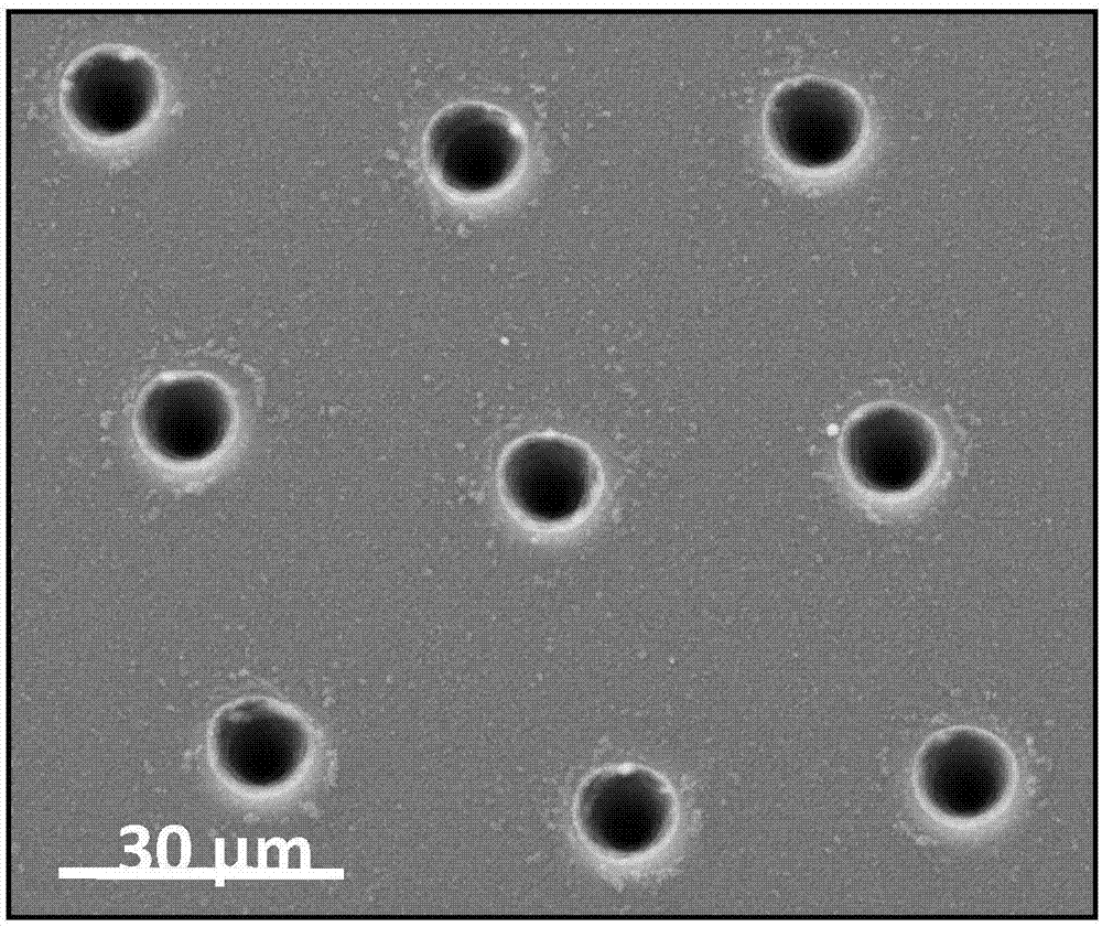
[0055] Then fix the cleaned 2-inch Si substrate on a two-dimensional electric translation stage, use a pulsed laser with a wavelength of 355nm, a pulse interval of 40ns, and a pulse repetition frequency of 1KHz, and converge the laser spot with a 20x objective lens so that its focus is The surface of the substrate material. Adjust the laser power to 0.08W to perform microhole ablation. After a microhole ablation is completed, move the displacement platform along a fixed direction (x direction) with the distance set at 30 μm, and then perform ablation of the next microhole, and repeat in turn. After the preparation of a row of microholes is completed, adjust the displacement platform in another direction (y direction), and also set the spacing to 30 μm, and repeat the ablation in sequence until the hole spacing of 3...

Embodiment 2

[0058] First utilize the UV spectrophotometer to measure the reflectivity of the cleaned 2-inch Si wafer, the results are as follows Figure 4 Shown at midline 1.

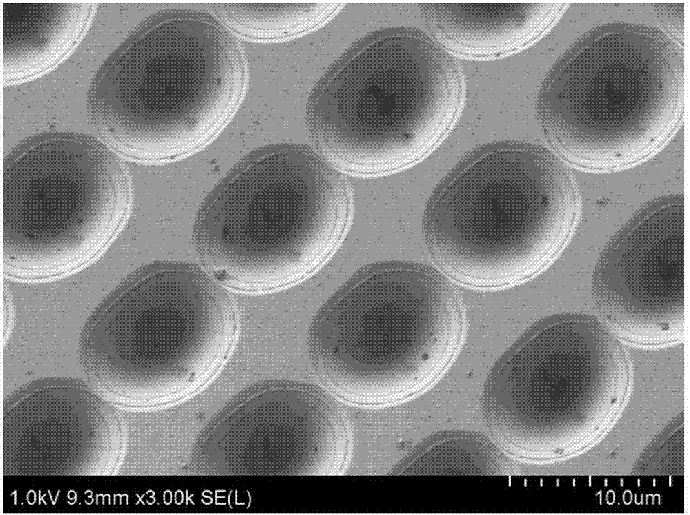
[0059] Then fix the cleaned 2-inch Si substrate on a two-dimensional electric translation stage, use a pulsed laser with a wavelength of 355nm, a pulse interval of 40ns, and a pulse repetition frequency of 1KHz, and converge the laser spot with a 20x objective lens so that its focus is The surface of the substrate material. Adjust the laser power to 0.08W to perform microhole ablation. After a microhole ablation is completed, move the displacement platform along a fixed direction (x direction) with the distance set at 15 μm, and then perform ablation of the next microhole, and repeat in turn. After the preparation of a row of microholes is completed, adjust the displacement platform in another direction (y direction), and also set the spacing to 15 μm, and repeat the ablation in sequence until the hole spacing of ...


PUM

PropertyMeasurementUnit
pore sizeaaaaaaaaaa
diameteraaaaaaaaaa
transmittivityaaaaaaaaaa

Abstract

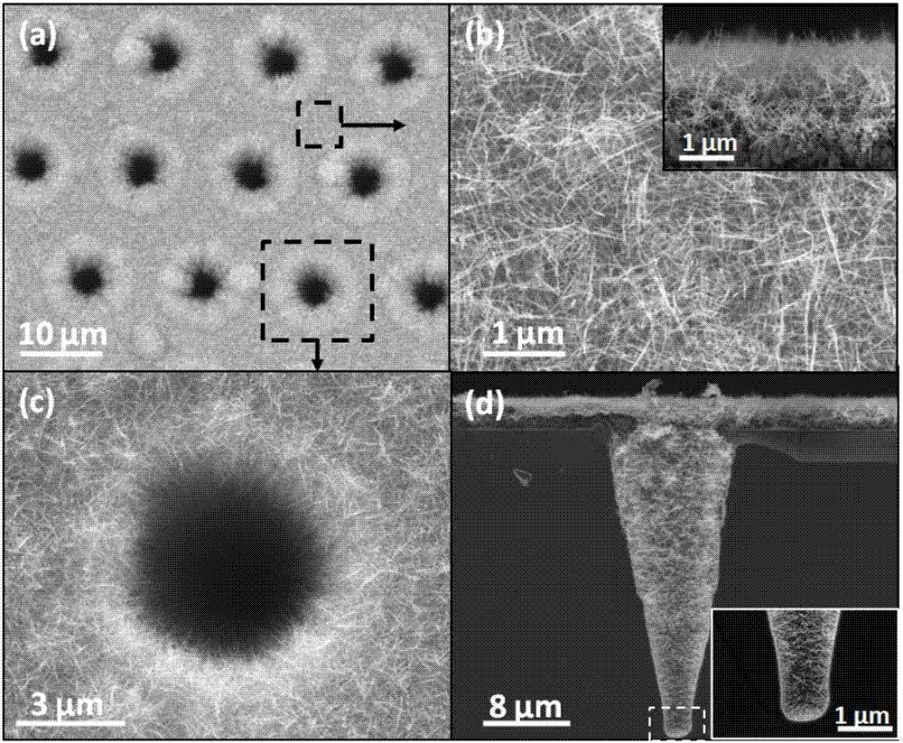
The invention discloses an ultra-wideband anti-reflection film and a preparation method thereof. The ultra-wideband anti-reflection film comprises a substrate, wherein a micropore array is formed in the surface of the substrate, and a layer of ITO nanowire thin film is prepared on the micropore array. According to the ultra-wideband anti-reflection film and the preparation method thereof, micropore structures arranged at certain intervals are prepared on the surface of the substrate by utilizing a laser micro-machining technology, and the layer of ITO nanowire thin film is prepared on the micropore structures and covers the micropore array completely. The prepared ultra-wideband anti-reflection film has good permeability and good electrical conductivity, and achieves the effective anti-reflection in400-2500 nm bands (bandwidth greater than 5). Through processing the surface of a solar cell, the preparation method disclosed by the invention realizes anti-reflection of a spectrum with in an ultra-wideband range by utilizing the micropore array combined with the novel nanowire material, and provides an efficient industrial preparation method for improving efficiency of the solar cell.

Description

technical field [0001] The invention relates to the field of solar cell anti-reflection film, in particular to a solar cell anti-reflection film and a preparation method thereof. Background technique [0002] With the development of the solar cell industry, improving the efficiency of solar cells has attracted great attention in recent years. In order to improve the conversion efficiency of solar cells, the surface of solar cells must have a strong anti-reflection capability, so that more sunlight can be absorbed. Therefore, antireflective coatings have been extensively studied and applied. [0003] The traditional anti-reflection coating (anti-reflection coating) is composed of a single-layer film with a thickness of 1 / 4 wavelength. Within the range, it cannot play a good anti-reflection effect, resulting in very low conversion efficiency of solar cells. In theory, graded-refractive-index coatings can be used to achieve broad-band anti-reflection, but the preparation of ...

Claims


Application Information

Patent Timeline
Patent Type & Authority Applications(China)
IPC IPC(8): H01L31/0216B82Y20/00B82Y40/00B82Y30/00
CPCB82Y20/00B82Y30/00B82Y40/00H01L31/02168Y02E10/50
Inventor 李强王帅云峰
Owner XI AN JIAOTONG UNIV
Learn More