Compound semiconductor thermoelectric material and method for manufacturing same

A technology of thermoelectric materials and semiconductors, which is applied in the manufacture/processing of thermoelectric devices, junction lead-out materials of thermoelectric devices, components of thermoelectric devices, etc. Large-scale production and other issues, to achieve the effect of reducing thermal conductivity and high-efficiency thermoelectric cooling

Active Publication Date: 2017-11-28
LG CHEM LTD
View PDF6 Cites 3 Cited by
  • Summary
  • Abstract
  • Description
  • Claims
  • Application Information

AI Technical Summary

Problems solved by technology

[0007] However, in most cases, although the dispersion of nm-scale fine particles for phonon scattering is effective in reducing the lattice thermal conductivity, it tends to greatly reduce the electrical conductivity
Furthermore, the fabrication of this thermoelectric material requires the use of costly processes for the fabrication and dispersion of nm-scale fine particles, which are not suitable for large-scale production

Method used


Image

  • Compound semiconductor thermoelectric material and method for manufacturing same
  • Compound semiconductor thermoelectric material and method for manufacturing same
  • Compound semiconductor thermoelectric material and method for manufacturing same

Examples


experiment example

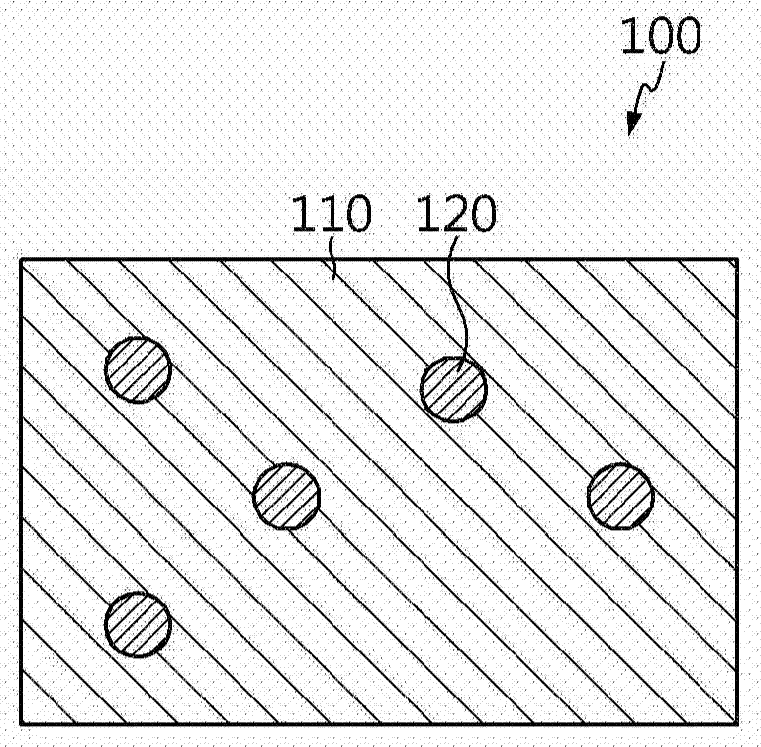
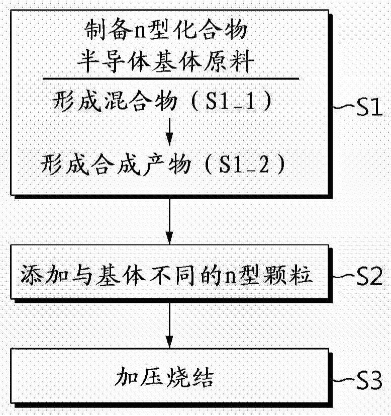
[0096] The reactants Bi, Te and Se pellets were prepared and ground, and mixed using a hand mill to produce Bi 2 Te 2.68 Se 0.32 The composition of the mixture (BTS material). Those containing added metal powders, especially Zn and / or Cu, were prepared to tune the properties of the Bi-Te-Se system. Furthermore, the mixture was put into a quartz tube and sealed under vacuum to produce an ampoule, and the ampoule was placed in a tube furnace, followed by heat treatment at a temperature of 400° C. for 12 hours.

[0097] The powder synthesized by the heat treatment was pulverized / classified using a sieve with a mesh size of 75 μm.

[0098] To prepare InSb and InSb:Se materials to be used as n-type particles, In, Sb and Se pellets were each loaded into a quartz tube and sealed under vacuum. Se is added in an amount of 0.1 mol % relative to InSb. Melting was carried out in a quartz tube in a furnace at 600° C. for 10 minutes, followed by air cooling. The ingot produced by melt...


PUM

PropertyMeasurementUnit
particle sizeaaaaaaaaaa
electrical conductivityaaaaaaaaaa
size distributionaaaaaaaaaa

Abstract

Provided are: a compound semiconductor thermoelectric material, having excellent thermoelectric conversion performance by having an excellent power factor and ZT value, and in particular, having excellent thermoelectric conversion performance at a low temperature; a method for manufacturing the same; and a thermoelectric module, a thermoelectric generator, or a thermoelectric cooling device, etc. using the same. The compound semiconductor thermoelectric material according to the present invention comprises: an n-type compound semiconductor matrix; and n-type particles which are dispersed in the matrix, are compound semiconductors which are different from the matrix, and have an average particle diameter of 1 micrometer to 100 micrometers.

Description

technical field [0001] The present disclosure relates to a compound semiconductor and a method of manufacturing the same, and more particularly, to a compound semiconductor thermoelectric material having excellent thermoelectric conversion performance and which can be effectively applied to a thermoelectric conversion element and a method of manufacturing the same. This application claims priority from Korean Patent Application No. 10-2015-0103215 filed in the Republic of Korea on Jul. 21, 2015, the disclosure of which is incorporated herein by reference. Background technique [0002] Compound semiconductors are semiconductors composed of two or more elements instead of one element (for example, silicon or germanium). Various types of compound semiconductors have been developed and are currently being used in various industrial fields. In general, compound semiconductors can be used for thermoelectric conversion elements, light emitting devices (for example, light emitting ...

Claims


Application Information

Patent Timeline
Patent Type & Authority Applications(China)
IPC IPC(8): H01L35/16H01L35/18H01L35/34
CPCH10N10/852H10N10/853H10N10/01H10N10/80
Inventor 权五贞崔铉祐林炳圭郑明珍朴哲熙
Owner LG CHEM LTD
Why Eureka
Try Eureka