Regeneration and purification process of recyclable silicon material in photovoltaic industry chain

An industrial chain and silicon material technology, which is applied in the field of recycling and purification of recyclable silicon material in the photovoltaic industry chain, can solve the problems of inability to process recycled silicon material, unstable battery, and high decay rate, and achieve rapid separation, improve utilization, and improve quality effect

Active Publication Date: 2017-12-01
YIXING YUYUAN ENERGY EQUIP TECH DEV
View PDF3 Cites 3 Cited by
  • Summary
  • Abstract
  • Description
  • Claims
  • Application Information

AI Technical Summary

Problems solved by technology

In order to reduce costs, some enterprises doped some recycled silicon materials into high-purity silicon for ingot casting, resulting in defects such as battery

Method used


Image

  • Regeneration and purification process of recyclable silicon material in photovoltaic industry chain
  • Regeneration and purification process of recyclable silicon material in photovoltaic industry chain

Examples


Embodiment 1

[0059] The regeneration and purification process of reusable silicon material includes the following steps:

[0060] (1) Classification and cleaning

[0061] The silicon material recovered from the photovoltaic industry chain was screened with a resistance tester and manual cooperation, and the silicon material with a resistivity between 0.5 and 3Ω·cm was screened.

[0062] The above-mentioned selected silicon material is opened, the surface is mechanically polished, and the thickness of the surrounding and bottom skin is 0.1-8 mm, and the thickness of the top skin is 0.2-10 mm.

[0063] With volume ratio of 5:1:1 30wt% sulfuric acid, 28wt% H 2 O 2 The silicon material was soaked in a mixture of water and water for 15 minutes, and then 25wt% ammonia water and 28wt% H were used in a volume ratio of 5:1:1. 2 O 2 Soak in a mixture of water and water for 15 minutes.

[0064] The silicon material is re-cleaned by pure water through ultrasonic cleaning technology, and finally v...

Embodiment 2

[0074] This embodiment is basically the same as Embodiment 1, the difference is:

[0075] (1) In the classification and cleaning step, the silicon material with resistivity < 0.5 Ω·cm is screened out.

[0076] (2) The treatment time of the smelting and impurity removal process is 12h, and the amount of the electrophoresis agent added is 1 / 100 of the weight of the silicon material.

[0077] (3) The time for vacuum overflow, impurity removal, blowing and cooling treatment is 12h.

[0078] In this embodiment, the yield rate of silicon material that meets the solar-grade polysilicon standard is 71%.

Embodiment 3

[0080] This embodiment is basically the same as Embodiment 1, the difference is:

[0081] (1) The classification and cleaning step screen out the silicon material with resistivity > 3 Ω·cm.

[0082] (2) The treatment time of the smelting and impurity removal process is 4h, and the amount of the electrophoresis agent added is 1 / 400 of the weight of the silicon material.

[0083] (3) The time for vacuum overflow, impurity removal, blowing and cooling treatment is 4h.

[0084] In this embodiment, the yield rate of silicon material that meets the solar-grade polysilicon standard is 76%.

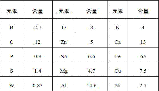
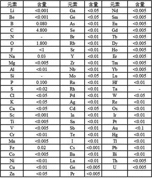
[0085] Table 1 and Table 2 show the content of impurity elements before and after the silicon material in Example 2 is purified.

[0086] Table 1 Content of polysilicon impurity elements before purification (ppmWt)

[0087]

[0088] Table 2 Purified polysilicon impurity element content (ppmWt)

[0089]


PUM

PropertyMeasurementUnit
Resistivityaaaaaaaaaa

Abstract

The invention discloses a regeneration and purification process of a recyclable silicon material in a photovoltaic industry chain. The recyclable silicon material in the photovoltaic industry chain is subjected to regeneration and purification to produce a silicon material which satisfies solar energy-grade standard. The process includes the steps of: 1) sorting and cleaning the recyclable silicon material; 2) smelting the silicon material to remove impurities; 3) performing vacuum overflow to remove impurities; and 4) classifying products. The process is environment-friendly, simple, energy-saving and low-cost. Yield of the silicon material, which satisfies the solar energy-grade standard, is higher than 70%; and purity of the silicon material is increased from 2-3 N to more than 6 N.

Description

technical field [0001] The invention relates to the technical field of photovoltaic silicon material recycling, in particular to a regeneration and purification process of recyclable silicon material in photovoltaic industry chain. Background technique [0002] According to the "Thirteenth Five-Year Plan for Solar Energy Development" issued by the National Energy Administration in 2016, the development goal of solar energy: by the end of 2020, the installed capacity of solar power will reach more than 110 million kilowatts, of which the installed capacity of photovoltaic power generation will reach more than 105 million kilowatts, and the annual utilization of solar energy will reach 105 million kilowatts. The amount reached more than 140 million tons of standard coal. In order to achieve the development goals of the "13th Five-Year Plan", it is necessary to purify ingot furnaces and ingot silicon materials or pull monocrystalline silicon materials to reach more than 1 milli...

Claims


Application Information

Patent Timeline
IPC IPC(8): C01B33/037C30B35/00
CPCC01B33/037C01P2006/80C30B35/007
Inventor 高文秀
Owner YIXING YUYUAN ENERGY EQUIP TECH DEV
Why Eureka
Try Eureka