Method for forming carbon/metal double-layer structure and carbon/metal/carbon triple-layer structure on substrate

A manufacturing method and metal layer technology, applied in metal material coating process, coating, ion implantation plating, etc., can solve problems such as limiting the application of graphene, inability to completely remove it, and reducing the sensitivity of graphene.

Inactive Publication Date: 2017-12-01
NAT KAOHSIUNG UNIV OF SCI & TECH
View PDF5 Cites 3 Cited by
  • Summary
  • Abstract
  • Description
  • Claims
  • Application Information

AI Technical Summary

Problems solved by technology

This layer of organic macromolecules is mostly long-chain hydrocarbons without crystallization. Once this substance touches the surface of graphene, it cannot be completely removed. The organic macromolecules remaining on the surface of graphene will shield graphene and Environmental exposure reduces the sensitivity of graphene to environmental changes and limits the application of graphene in sensors

Method used


Image

  • Method for forming carbon/metal double-layer structure and carbon/metal/carbon triple-layer structure on substrate
  • Method for forming carbon/metal double-layer structure and carbon/metal/carbon triple-layer structure on substrate
  • Method for forming carbon/metal double-layer structure and carbon/metal/carbon triple-layer structure on substrate

Examples


Embodiment Construction

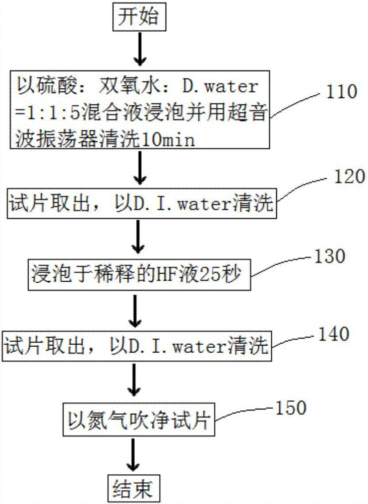
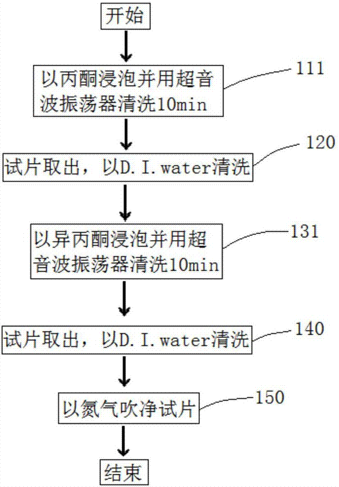
[0045] In the following embodiments, the present invention discloses a low-temperature manufacturing (amorphous) crystalline carbon single-component layer, (amorphous) crystalline carbon / copper or nickel layer double-component layer, (amorphous) crystalline carbon / copper or nickel layer and (Amorphous) crystalline phase carbon / copper layer / (amorphous) crystalline phase carbon three-component layering method. The crystalline carbon (crystal carbon) refers to the regular arrangement of carbon atoms, and the amorphous carbon refers to amorphous carbon.

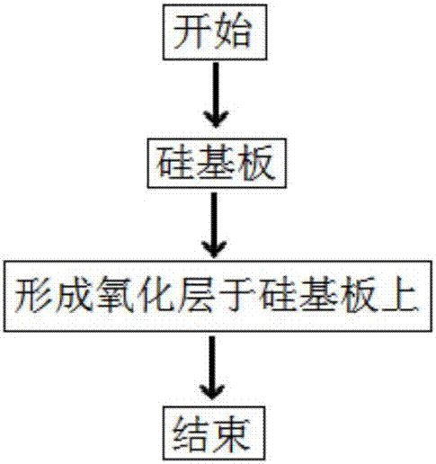
[0046] The substrate of the present invention may be a silicon substrate, a glass substrate, a quartz substrate, or a PET substrate, and the PET film here is a high-temperature-resistant (up to 350° C.) polyester film. Glass substrates are also substrates that can withstand high temperatures (up to 550°C).

[0047] Silicon substrate pre-cleaning such as Figure 1A shown. As shown in step 100, the silicon substrate is soaked in ...


PUM

PropertyMeasurementUnit
thicknessaaaaaaaaaa

Abstract

The invention discloses a method for forming a carbon / metal double-layer structure and a carbon / metal / carbon triple-layer structure on a substrate. The method comprises the steps of: 1) performing a nickel sputtering process, wherein a nickel target is bombarded with plasma so as to deposit a copper or nickel layer onto the substrate; 2) bombarding a carbon-containing reaction gas as well as a copper or a nickel target with plasma so as to form a copper, or nickel, and carbon mixed layer on the nickel layer; 3) performing a vacuum annealing process to form a (non)-crystalline-phase carbon / copper or nickel layer / (non)-crystalline-phase carbon / copper or nickel layer structure on the substrate. In another embodiment, the method includes the steps of: 1) pre-sputtering a nickel layer in a sputtering chamber; 2) simultaneously or successively bombarding a copper or nickel target and a graphite target with plasma and then performing annealing in a hydrogen-containing atmosphere so as to form a (non)-crystalline-phase carbon / copper or nickel layer / (non)-crystalline-phase carbon triple-layer structure.

Description

technical field [0001] The present invention relates to a low-temperature manufacturing method of carbon single-component layer, or carbon-copper double-layer or carbon-copper-carbon three-layer, especially relates to a substrate that is subjected to plasma bombardment of copper and carbon-containing reaction gas at a temperature below room temperature to 400°C. Or the copper target and the graphite target are bombarded at the same time or in a predetermined order, and then annealed at a predetermined temperature or not annealed to form the target product for industrial use. Background technique [0002] Perfect graphene refers to a thin film with a single carbon atomic layer thickness and a regular hexagonal lattice structure formed by carbon atoms covalently bonded to each other in sp2 mixed orbital domains along a plane. Graphene is known to have excellent carrier mobility (5000-10000cm 2 / Vs), hardness (1050Gpa), thermal conductivity (5000W / mk), current carrying capacit...

Claims


Application Information

Patent Timeline
Patent Type & Authority Applications(China)
IPC IPC(8): C23C14/14C23C14/34C23C14/58C23C14/06
CPCC23C14/06C23C14/14C23C14/34C23C14/3457C23C14/3464C23C14/5806
Inventor 赖富德
Owner NAT KAOHSIUNG UNIV OF SCI & TECH
Why Eureka
Try Eureka