

Etching solution composition for silver-containing layer and a display substrate using the same
A technology for display substrates and compositions, applied in the direction of surface etching compositions, optics, instruments, etc., can solve the problems of poor wiring side profile, difficulty in fine etching, increased silver re-adsorption, etc., to maintain etching uniformity, excellent Etching uniformity, anti-resorption effect
- Summary
- Abstract
- Description
- Claims
- Application Information
AI Technical Summary
Problems solved by technology
Method used
Image

Examples
experiment example
[0073] Performance test of etching solution composition
[0074] Indium oxide film / silver film / indium oxide film are sequentially coated on the substrate to form a three-layer film, and a photoresist with a predetermined pattern is formed on the substrate through a photolithography process to prepare a test piece. Thereafter, an etching process was performed on the indium oxide film / silver film / indium oxide film using the compositions of Examples 1 to 8 and Comparative Examples 1 to 12, respectively.
[0075] Put the etching solution compositions of the above-mentioned Examples 1-8 and Comparative Examples 1-12 into the experimental equipment of the jet etching method (model name: ETCHER (TFT), K.C.Tech Company), and set the temperature to 40°C while heating. After that, when the temperature reached 40±0.1° C., the above-mentioned etching process of the test piece was carried out. Regarding the total etching time, it was carried out in accordance with the process time carri...
experiment example 1
[0076] Experimental example 1. Measurement of side erosion distance of etching solution composition
[0077] Afterwards, the substrate is put in and sprayed, and the etched substrate is taken out, washed with deionized water, and then dried. The dried substrate was cut, and the cross section was confirmed with a scanning electron microscope (SEM, model name: SU-8010, manufactured by Hitachi Corporation).
[0078] As a standard for measuring the side etch distance, the width from the edge of the photoresist to the inside of the etched metal was measured, and the results are shown in Table 2 below.
[0079]
[0080] ◎: very good (side erosion ≤ 0.1μm)
[0081] ○: Excellent (0.1μm<undercut≤0.2μm)
[0082] △: Good (0.2μm
[0083] Ⅹ: Poor (side etching>0.3μm)
experiment example 2
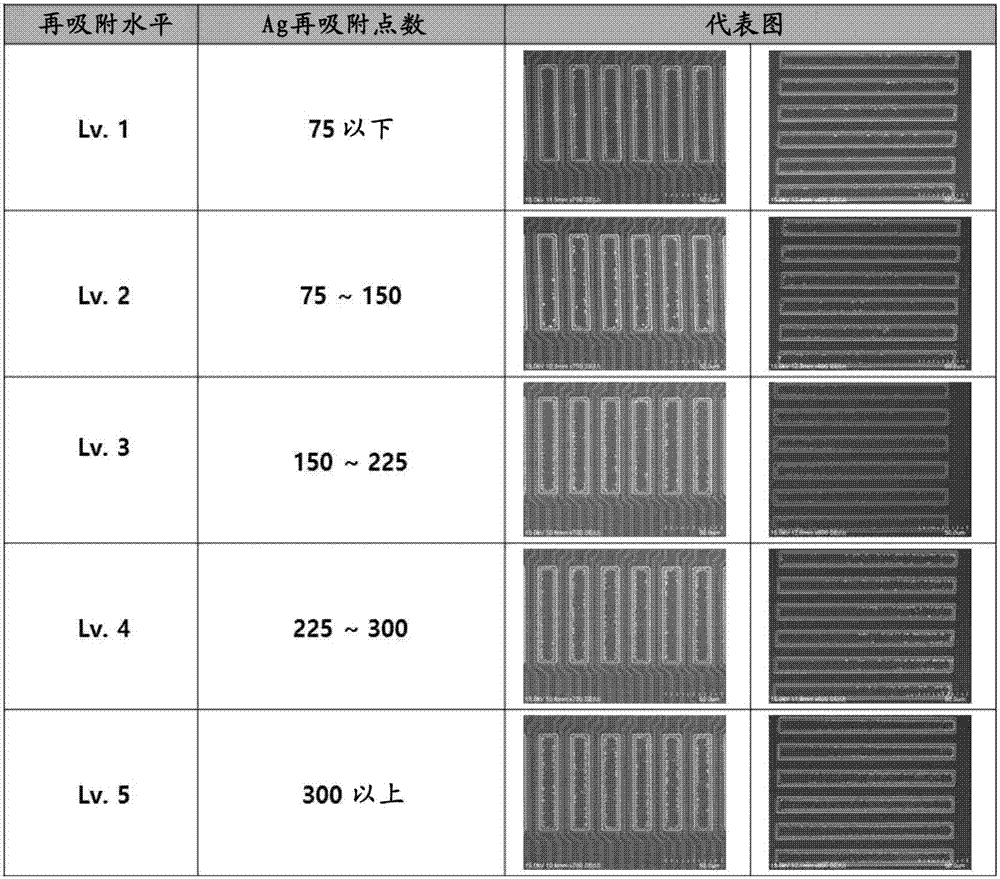
[0084] Experimental example 2. Silver re-adsorption measurement
[0085] Afterwards, the substrate was put in and sprayed, and when the etching time reached 100 seconds, the substrate was taken out and washed with deionized water. After that, it is dried with a hot air drying device, and the photoresist is removed with a photoresist stripper (PR stripper). After washing and drying, use a scanning electron microscope (SEM, model name: SU-8010, manufactured by Hitachi Corporation) to examine the specific parts where friction may occur mainly at parts where dissimilar metals such as data wiring are exposed or due to bending phenomena after etching. The phenomenon that etched silver (Ag) is adsorbed on the part is analyzed by observing the whole surface. pass figure 1 and the following criteria were evaluated, and the results are shown in Table 2 below.
[0086]
[0087] ◎: Excellent (less than 50)
[0088] ○: Excellent (below 80)
[0089] △: Good (less than 100 pieces) ...
PUM
 Abstract
Description
Claims
Application Information