5G communication 20GHz laser dual chip package base and method of manufacture

A technology for packaging bases and lasers, used in lasers, laser parts, semiconductor lasers, etc., can solve problems such as high cost and affect the 5G communication process, and achieve the effect of solving heat dissipation problems, promoting the speed of popularization, and realizing miniaturization.

Inactive Publication Date: 2017-12-15
GUANGDONG GASTIGHT HERMETICAL COMPONENT
View PDF3 Cites 13 Cited by
  • Summary
  • Abstract
  • Description
  • Claims
  • Application Information

AI Technical Summary

Problems solved by technology

[0002] With the continuous development of optical fiber communication technology and the advent of the era of big data, the communication capacity and bandwidth continue to expand, and Gigabit networks will gradually enter thousands of households. However, due to the limitation of high-speed optical devices (40GHz and above) Due to the limitations of TO packaging, butterfly-shaped (BTF) packaging is currently used. Due to the use of microwave circuit design and large cavity space, the butterfly-shaped laser has excellent performance, but the cost is high. The current single-chip TO The packaging structure is difficult to break through the bottleneck of 40GHz, which affects the process of 5G communication in a certain sense

Method used


Image

  • 5G communication 20GHz laser dual chip package base and method of manufacture
  • 5G communication 20GHz laser dual chip package base and method of manufacture
  • 5G communication 20GHz laser dual chip package base and method of manufacture

Examples


Embodiment 1

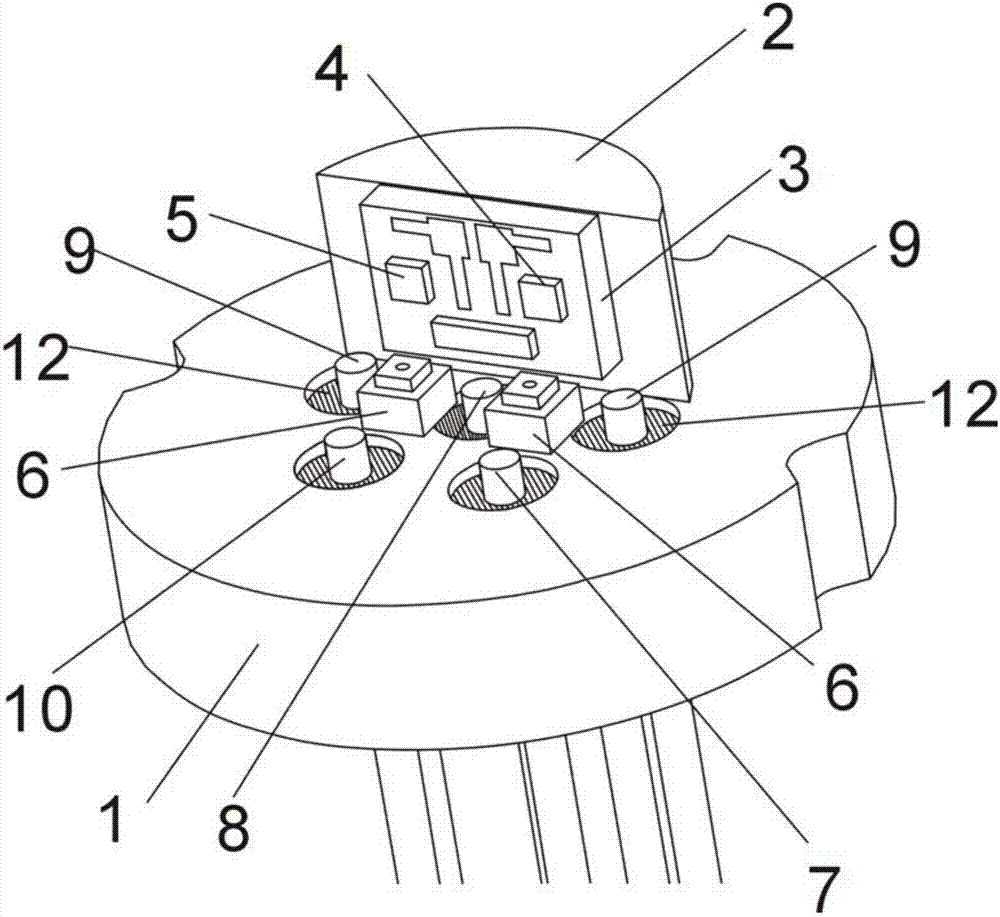
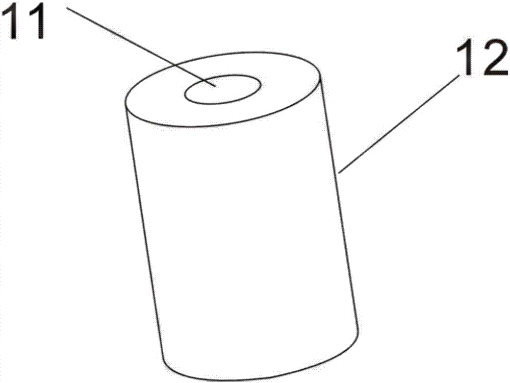
[0031] See figure 1 , 2 Said, a 5G communication 20GHz laser double-chip packaging base, including a base body 1, a support 2 is installed on the base body 1, a printed circuit board 3 is installed in the support 2, the The printed circuit board 3 is provided with a first laser chip 5 and a second laser chip 4. The printed circuit board 3 is printed with silver paste for a hybrid microwave circuit and printed with a Peltier paste for a TEC circuit. The two are used for laser input current. The monitored detector PD 6 is installed on the base body, and the base body 1 is also equipped with a 50-ohm high-speed modulation electrical signal input pin 9, a detector PD input pin 10, and an input pin 7 of the TEC circuit. 1. Ground output pin 8; said 50 ohm high-speed modulation electrical signal input pin 9 has two, set for the coaxial structure. The 50 ohm high-speed modulation electrical signal input pin 9, the detector PD input pin 10, the input pin 7 of the TEC circuit, and th...

Embodiment 2

[0038] A method for manufacturing a 5G communication 20GHz laser double-chip packaging base, the method comprising:

[0039] (1) Base body: made of No. 10 carbon steel, which is precision stamped and formed, and nickel-plated with 3-5 microns after degreasing and cleaning;

[0040] (2) Support: Oxygen-free copper, nickel-plated 3-5 microns, 85-15 silver-copper solder with a thickness of 0.1 mm, welded on the base body;

[0041] (3) Printed circuit board: use high thermal conductivity aluminum nitride substrate, length and width 1.5 mm, height 0.8 mm, thickness 0.3 mm; set the first laser chip and the second laser chip, and print the hybrid microwave circuit with silver paste. Ertier paste printing TEC circuit;

[0042] (4) Glass insulators: HYG9 series low-loss, low-dielectric constant glass press-molded plain-fired glass insulators are used;

[0043] (5) Input pin: 50 ohm high-speed modulation electrical signal input pin, the material is made of 4J50 iron-nickel alloy, proc...


PUM


Abstract

The invention discloses a 5G communication 20GHz laser dual chip package base, which comprises a base body. A supporting member is arranged on the base body. A printed circuit board is arranged in the supporting member. A first laser chip and a second laser chip are arranged on the printed circuit board. The printed circuit board is printed with a hybrid microwave circuit with silver paste and a TEC circuit with Peltier paste. Two detectors PD for laser input current monitoring are mounted on the base body. The base body is also equipped with 50 ohm high-speed modulation electrical signal input pins, a detector PD input end pin, a TEC circuit input end pin and a ground output pin therein. The invention also discloses a preparation method thereof. According to the invention, the 40 GHz bandwidth for the single laser TO package is achieved. Thus, the cost is greatly reduced, the purpose of miniaturization is achieved, the compatibility with existing optical device standards is also achieved, and the popularity of the 5G network of high-speed optical devices is effectively promoted.

Description

technical field [0001] The invention belongs to the field of semiconductor laser packaging components, in particular to a 5G communication 20GHz laser double-chip packaging base and a manufacturing method thereof. Background technique [0002] With the continuous development of optical fiber communication technology and the advent of the era of big data, the communication capacity and bandwidth continue to expand, and Gigabit networks will gradually enter thousands of households. However, due to the limitation of high-speed optical devices (40GHz and above) Due to the limitations of TO packaging, butterfly-shaped (BTF) packaging is currently used. Due to the use of microwave circuit design and large cavity space, the butterfly-shaped laser has excellent performance, but the cost is high. The current single-chip TO The packaging structure is difficult to break through the bottleneck of 40GHz, which affects the process of 5G communication in a certain sense. Contents of the ...

Claims


Application Information

Patent Timeline
Patent Type & Authority Applications(China)
IPC IPC(8): H01S5/022H01S5/024H01S5/042
CPCH01S5/02212H01S5/02415H01S5/042
Inventor 温演声
Owner GUANGDONG GASTIGHT HERMETICAL COMPONENT
Why Eureka
Try Eureka