Semiconductor device and method of forming the same

A semiconductor and device technology, which is applied in the field of semiconductor devices and their formation, can solve the problems that the electrical performance of semiconductor devices needs to be improved, and achieve the effect of improving the response delay of electrical signals and shortening the transmission path of electrical signals

Active Publication Date: 2020-03-10
SEMICON MFG INT (SHANGHAI) CORP +1
View PDF5 Cites 0 Cited by
  • Summary
  • Abstract
  • Description
  • Claims
  • Application Information

AI Technical Summary

Problems solved by technology

[0004] Although the introduction of high-k metal gates can improve the electrical performance of semiconductor devices to a certain extent, the electrical performance of semiconductor devices formed by the prior art still needs to be improved.

Method used


Image

  • Semiconductor device and method of forming the same
  • Semiconductor device and method of forming the same
  • Semiconductor device and method of forming the same

Examples


Embodiment Construction

[0020] It can be seen from the background art that the electrical performance of the semiconductor devices formed in the prior art needs to be improved, for example, the yield rate of the semiconductor devices formed in the prior art is low, and the problem of electrical signal response delay is significant.

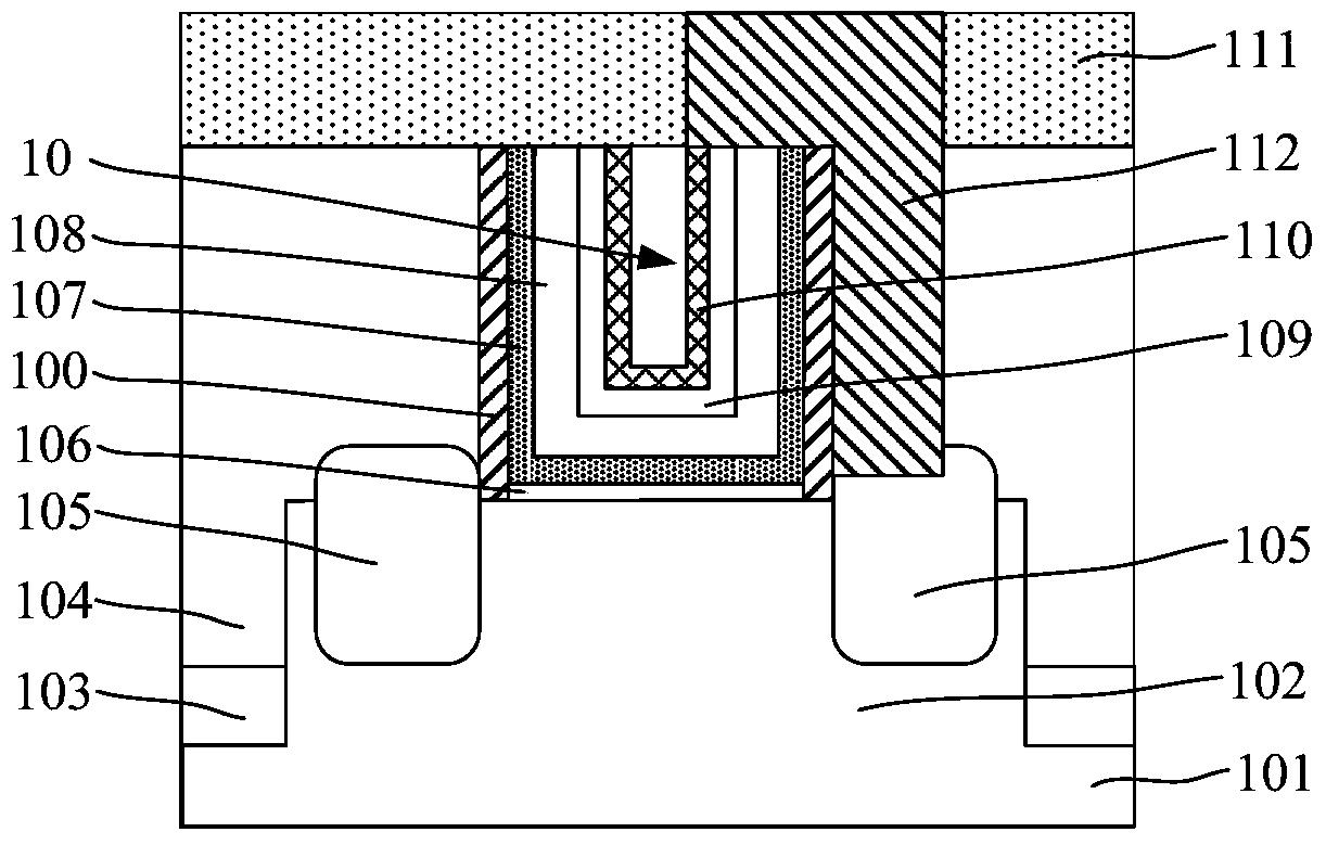
[0021] refer to figure 1 , figure 1 It is a schematic cross-sectional structure diagram of a PMOS transistor, and the PMOS transistor may be a part of an SRAM device. The PMOS tube includes:

[0022]The substrate 101, the fin 102 on the substrate 101, the isolation layer 103 on the substrate 101 and covering part of the sidewall of the fin 102; the gate structure across the fin 102, and the gate structure covers the fin Part of the top and sidewall of the portion 102, wherein the gate structure includes: an interface layer 106, a high-k gate dielectric layer 107 on the interface layer 106, a P-type work function layer 108 on the high-k gate dielectric layer 107 , an N...


PUM

PropertyMeasurementUnit
thicknessaaaaaaaaaa
thicknessaaaaaaaaaa
thicknessaaaaaaaaaa

Abstract

A semiconductor device and a formation method thereof are disclosed. The formation method of the semiconductor device comprises the following steps of carrying out back etching to remove a P-type work function layer and an N-type work function layer with a first thickness on a first opening sidewall of a PMOS region; forming a cap layer on the N-type work function layer of the second opening, wherein the cap layer is located on the N-type work function layer and the P-type work function layer in the first opening after back etching; forming a first metal layer used for filling the first opening and the second opening on the cap layer; forming a top dielectric layer on the first metal layer and an interlayer dielectric layer; and forming a contact through hole passing through the top dielectric layer and the interlayer dielectric layer, wherein the contact through hole exposes a top of the first metal layer in the PMOS region and a top of a first source and drain doping region on one side of the first opening. In the invention, an electric signal response delay problem is improved so that electric performance of the formed semiconductor device is improved.

Description

technical field [0001] The invention relates to the technical field of semiconductor manufacturing, in particular to a semiconductor device and a forming method thereof. Background technique [0002] The main semiconductor device of an integrated circuit, especially a very large scale integrated circuit, is a metal-oxide-semiconductor field effect transistor (MOS transistor). With the continuous development of integrated circuit manufacturing technology, the technology nodes of semiconductor devices are continuously reduced, and the geometric dimensions of semiconductor structures are continuously reduced following Moore's law. When the size of the semiconductor structure is reduced to a certain extent, various secondary effects caused by the physical limit of the semiconductor structure appear one after another, and it becomes more and more difficult to scale down the feature size of the semiconductor structure. Among them, in the field of semiconductor manufacturing, the ...

Claims


Application Information

Patent Timeline
Patent Type & Authority Patents(China)
IPC IPC(8): H01L21/8238H01L29/51
CPCH01L21/823857H01L29/51
Inventor 李勇
Owner SEMICON MFG INT (SHANGHAI) CORP
Why Eureka
Try Eureka