Epitaxial layer structure of metal-oxide channel semiconductor field effect transistor

A technology of field-effect transistors and oxide semiconductors, applied in semiconductor devices, electrical components, circuits, etc., can solve problems such as inability to optimize channel power MOSFET devices, achieve improved reliability, improved withstand voltage capability, and reduced system resistance Effect

Inactive Publication Date: 2018-01-05
HUNTECK SEMICON (SHANGHAI) LTD
View PDF3 Cites 4 Cited by
  • Summary
  • Abstract
  • Description
  • Claims
  • Application Information

AI Technical Summary

Problems solved by technology

[0003] However, the single epitaxial layer or double epitaxial layer used in the trench MOSFET (Metal-Oxide Semiconductor Field Effect Transistor) used in the past has been unable to maximize the optimization of the channel power MOSFET device as the channel becomes deeper and denser. Performance

Method used


Image

  • Epitaxial layer structure of metal-oxide channel semiconductor field effect transistor
  • Epitaxial layer structure of metal-oxide channel semiconductor field effect transistor
  • Epitaxial layer structure of metal-oxide channel semiconductor field effect transistor

Examples


Embodiment Construction

[0034] In order to make the object, technical solution and advantages of the present invention clearer, the technical solution of the present invention will be described below in conjunction with the accompanying drawings and the embodiments thereof.

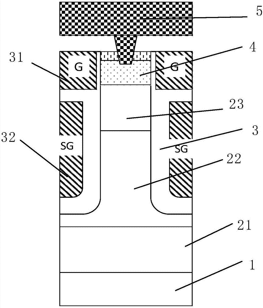
[0035] figure 1 Showing a specific embodiment of the present invention, a schematic longitudinal cross-sectional view of a metal-oxide channel semiconductor field effect transistor device. The metal-oxide channel semiconductor field effect transistor (channel power MOSFET) can be further divided into P channel and N channel devices according to the conduction channel; The depletion type when there is a conduction channel between the drain and the source and the enhancement type when the gate voltage is greater than (less than) zero. In the present invention, the power MOSFET is mainly an N-channel enhancement type (but not limited to an N-channel MOSFET, and the same implementation is also applicable to a P-channel MOSFET). Sp...


PUM


Abstract

The invention discloses an epitaxial layer structure of a metal-oxide channel semiconductor field effect transistor. The metal-oxide channel semiconductor field effect transistor is provided with an epitaxial layer structure, a gate, a substrate and a channel; a direction along the substrate towards the gate is defined as an extension direction; and the doping concentration of the epitaxial layerstructure is gradually increased and then gradually decreased in the extension direction. By virtue of the epitaxial layer structure, the voltage withstand performance of a metal-oxide channel semiconductor field effect transistor device can be improved, the on resistance can be lowered and reliability can be reinforced, so that the channel density of the metal-oxide channel semiconductor field effect transistor device is further improved and the unit cell dimension is reduced.

Description

technical field [0001] The invention belongs to the technical field of field effect transistors, in particular to an epitaxial layer structure of a metal-oxide channel semiconductor field effect transistor. Background technique [0002] A metal-oxide semiconductor field effect transistor is a field effect transistor that uses the effect of an electric field to control a semiconductor by using the gate of a metal layer across an oxide layer. It is widely used in analog circuits and digital circuits. With the advancement of semiconductor technology, high-density deep channel structures become possible, thereby further reducing the size of the device unit cell. In semiconductor processing, an epitaxial layer is a single crystal of silicon grown on a substrate. [0003] However, the single epitaxial layer or double epitaxial layer used in the trench MOSFET (Metal-Oxide Semiconductor Field Effect Transistor) used in the past has been unable to maximize the optimization of the ch...

Claims


Application Information

Patent Timeline
Patent Type & Authority Applications(China)
IPC IPC(8): H01L29/06H01L29/78H01L29/772
CPCH01L29/0878H01L29/7813H01L29/407H01L29/1045H01L29/66712H01L29/7827H01L29/0607H01L29/66666H01L29/0611H01L29/0615H01L29/66477
Inventor 胡军罗志云王飞
Owner HUNTECK SEMICON (SHANGHAI) LTD
Why Eureka
Try Eureka