Booster circuit and inverter topology with cascade diode circuit

A boost circuit and diode technology, applied in the field of improved topology, PFC boost circuit, power factor correction boost circuit, and power module, can solve the problems of high manufacturing cost of conventional circuits, and achieve improved switching characteristics and reverse recovery charge The effect of reducing and improving efficiency

Active Publication Date: 2018-01-05
VINCOTECH
View PDF3 Cites 3 Cited by
  • Summary
  • Abstract
  • Description
  • Claims
  • Application Information

AI Technical Summary

Problems solved by technology

Figure 8 to Figure 10 shows a conventional topology for a mixed voltage NPC inverter module, where the diodes need to commutate half of the DC voltage, but must block the full voltage during the inactive half-wave
In other words, fast diodes with high voltage ratings are required, whereby conventional circuits are expensive to manufacture

Method used


Image

  • Booster circuit and inverter topology with cascade diode circuit
  • Booster circuit and inverter topology with cascade diode circuit
  • Booster circuit and inverter topology with cascade diode circuit

Examples


Embodiment Construction

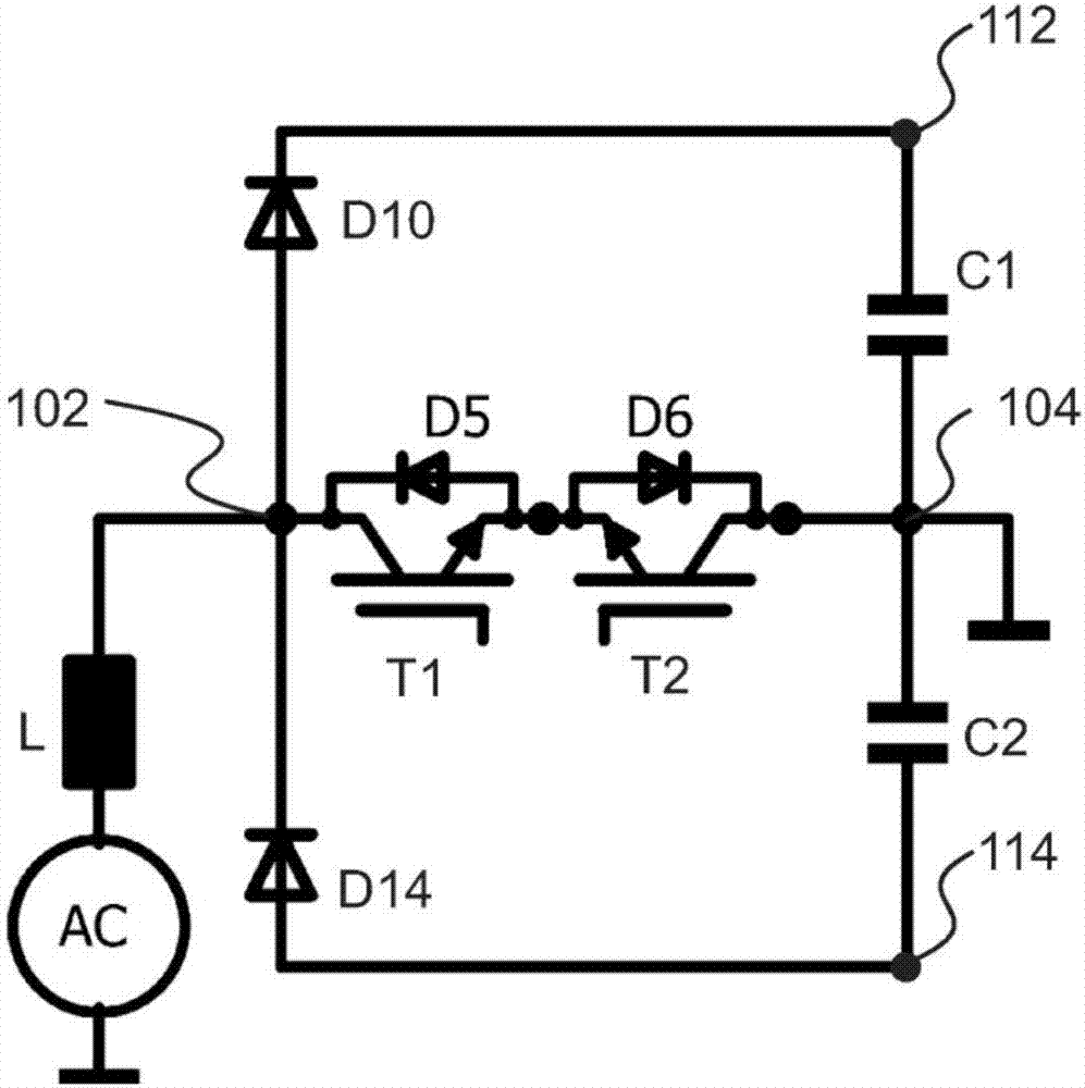
[0059] The invention will now be explained in more detail with reference to the accompanying drawings. refer to figure 1 , reference will first be made to a conventional neutral boost power factor correction (PFC) circuit in order to better understand the basic principles of the invention. The neutral boost PFC circuit uses a first input node 102 via an inductor L to connect to an alternating current power supply AC. The first transistor T1 and the second transistor T2 are connected in series between the first input node 102 and the second input node 104 connected to a reference potential, eg ground. In the illustrated embodiment, transistors T1 and T2 comprise insulated gate bipolar transistors (IGBTs). Accordingly, each of transistors T1, T2 is connected in anti-parallel with diodes D5 and D6, respectively. However, it is obvious to a person skilled in the art that other semiconductor switches can be used instead of IGBTs, such as field-effect transistors FETs, such as me...


PUM


Abstract

The invention, as a whole, relates to topology used for a booster circuit, an inverter and a half-bridge circuit. A power factor correction (PFC) booster circuit used for being connected to an AC power supply includes: an AC input node (102) used for being connected to the AC power supply; a reference level node (104) used for being connected to a reference level; and at least a first and second power transistors, which are in series-opposing connection between the AC power supply and the reference level node, wherein the first power transistor (T1) is in reverse parallel connection with a first power diode (D5), and the second power transistor (T2) is in reverse parallel connection with a second power diode (D6). First diode circuits (D1, D2) are connected between the AC input node (102)and a positive output node (112), and include a series connection, different in recovery time, of a first diode element and a second diode element.

Description

technical field [0001] The present invention relates generally to power electronic switching circuits, and in particular to power modules employing two or more controlled switches. More specifically, the present invention provides improved topologies for boost circuits, inverters and half bridge circuits. [0002] In the field of power electronics and in many applications such as inverter modules for the solar market, efficiency is becoming more and more important and efficiency optimization has become a major design goal. Photovoltaic solar panels typically use a pulse width modulation (PWM) inverter to convert the direct current (DC) power generated by the solar cells into alternating current (AC) power that can be fed to the grid. Typical additional applications of these inverters include their use in uninterruptible power supplies (UPS), fuel cells and wind turbines. In addition, PWM inverters can be used to provide compensation for reactive loads, for harmonic cancellat...

Claims


Application Information

Patent Timeline
Patent Type & Authority Applications(China)
IPC IPC(8): H02M1/42H02M7/217H02M7/487H02M7/5387H02M3/07
CPCH02M1/4208H02M1/4225H02M7/487Y02B70/10
Inventor E·特梅西M·弗里施
Owner VINCOTECH
Why Eureka
Try Eureka