Eureka AIR delivers breakthrough ideas for toughest innovation challenges, trusted by R&D personnel around the world.

Semiconductor laser and manufacturing method therefor

A laser and semiconductor technology, applied in the structure of optical waveguide semiconductor, the structure of optical resonator, the structure of active area, etc., can solve the problems of space hole burning, generation of optical filament phenomenon, and high cost of chip preparation

Active Publication Date: 2018-01-19
CHANGCHUN INST OF OPTICS FINE MECHANICS & PHYSICS CHINESE ACAD OF SCI
View PDF8 Cites 12 Cited by
  • Summary
  • Abstract
  • Description
  • Claims
  • Application Information

AI Technical Summary

Problems solved by technology

However, the tapered amplifier of the Master Oscillator Power Amplifier (MOPA) cannot provide a feedback beam to the seed light source, which will lead to the accumulation of carriers in the tapered amplification region, causing space hole burning, exciting high-order transverse modes, and reducing the output beam quality; the tapered waveguide of the tapered laser will produce a filament phenomenon when working at high current, which will deteriorate the beam quality and hinder the improvement of brightness; the preparation of the grating structure of the distributed feedback semiconductor laser (DFB) generally requires secondary epitaxy or Technologies such as electron beam lithography lead to high chip preparation costs and low yields

Method used


Image

  • Semiconductor laser and manufacturing method therefor
  • Semiconductor laser and manufacturing method therefor
  • Semiconductor laser and manufacturing method therefor

Examples


Embodiment Construction

[0041] The following will clearly and completely describe the technical solutions in the embodiments of the present invention with reference to the accompanying drawings in the embodiments of the present invention. Obviously, the described embodiments are only some, not all, embodiments of the present invention. Based on the embodiments of the present invention, all other embodiments obtained by persons of ordinary skill in the art without making creative efforts belong to the protection scope of the present invention.

[0042] In order to make the above objects, features and advantages of the present invention more comprehensible, the present invention will be further described in detail below in conjunction with the accompanying drawings and specific embodiments.

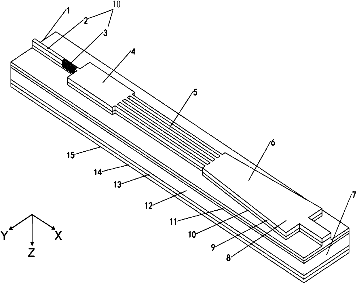
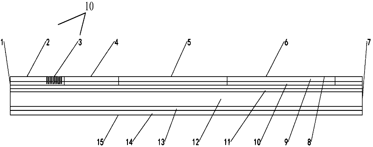
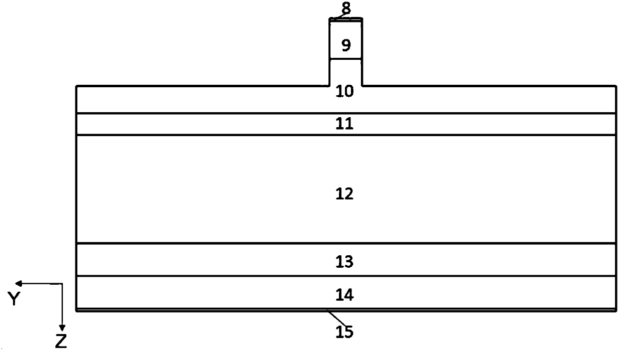
[0043] refer to Figure 1-Figure 7 , figure 1 A schematic structural diagram of a semiconductor laser provided by an embodiment of the present invention, figure 2 for figure 1 Side view of the semiconductor la...


PUM


Abstract

The invention discloses a semiconductor laser and a manufacturing method therefor, and the semiconductor laser comprises a substrate which is provided with a first surface and a second surface, whichare opposite to each other; a patterned epitaxial function layer which is located on the first surface, and is sequentially divided into a high-order optical grating coupling ridge waveguide, a lightbeam splitting waveguide, a ridge gain array waveguide and a self-organizing coherent beam combining waveguide in a first direction; The high-order optical grating coupling ridge waveguide generates asingle-frequency single-mode seed light source. The light beam splitting waveguide is located at one end of outgoing light of the high-order optical grating coupling ridge waveguide, and splits the seed light source into multiple laser paths. The ridge gain array waveguide is located at one end of outgoing light of the light beam splitting waveguide, and carries out the gain amplification of multiple laser paths. The self-organizing coherent beam combining waveguide is located at one end of the outgoing light of the ridge gain array waveguide, and carries out the coherent combination of multiple laser paths after gain amplification to form an output beam. According to the technical scheme of the invention, the semiconductor laser improves the light beam quality and brightness of the output beam.

Description

technical field [0001] The invention relates to the technical field of semiconductor devices, and more specifically, to a semiconductor laser and a manufacturing method thereof. Background technique [0002] Semiconductor lasers (LD) have many advantages such as small size, high efficiency, long life, and easy integration. High beam quality and narrow linewidth semiconductor lasers have higher beam quality, smaller slow axis divergence angle and narrower spectral linewidth, and are more suitable for large-scale semiconductor laser beam shaping and combining. It has wider application prospects in industry, military, medical and other aspects. Manufacture of semiconductor lasers with high power, high beam quality and narrow linewidth has always been the goal pursued by people. [0003] Although the traditional monolithic integrated semiconductor laser structure with high beam quality has made great progress in increasing output power and optimizing beam quality. However, th...

Claims


Application Information

Patent Timeline
Patent Type & Authority Applications(China)
IPC IPC(8): H01S5/12H01S5/22H01S5/34
Inventor 贾鹏陈泳屹秦莉张建伟宁永强王立军
Owner CHANGCHUN INST OF OPTICS FINE MECHANICS & PHYSICS CHINESE ACAD OF SCI
Why Eureka
Eureka Blog
Learn More