

A method for preparing niobium silicide coating on the surface of niobium or niobium alloy
A technology of niobium silicide and niobium alloy, which is applied in the coating process of metal materials, coating, molten spraying, etc., and can solve the problems of uneven coating thickness and structure, affecting the oxidation resistance of coatings, and poor thermal conductivity of powder mixtures. , to achieve the effects of controllable coating thickness, controllable coating composition and thickness, and strong chemical-metallurgical bonding
- Summary
- Abstract
- Description
- Claims
- Application Information
AI Technical Summary
Problems solved by technology
Method used
Image

Examples
preparation example Construction
[0023] Preparation of silicon coating. Specifically, silicon powder with a certain particle size distribution is selected, and the silicon powder is sprayed onto the surface of sandblasted niobium or niobium alloy by plasma spraying technology to form a silicon coating. The selected powder for spraying is silicon powder with a particle size of 10-120 μm, and the purity of the powder is greater than 98wt.%. Dry at 100-120°C for 1-3 hours and set aside. The process parameters of the plasma spraying technology may include: plasma gas Ar: 30-50 slpm; plasma gas H 2 : 6~15slpm; powder carrier gas Ar: 2~7slpm; spraying distance: 100~200mm; spraying power: 30~50kW; powder feeding rate: 10~30rpm. In the invention, by controlling the process parameters of the plasma spraying technology, the silicon powder is sprayed on the surface of the niobium or niobium alloy substrate to form a silicon coating with a thickness of 30-300 μm.
[0024] The substrate sprayed with the silicon coating...
Embodiment 1
[0032] A niobium silicide coating on a niobium metal surface, the preparation of which comprises the steps of:
[0033] 1) Sandblasting the surface of the Nb substrate with a sandblasting pressure of 0.4 MPa, ultrasonicating twice in absolute ethanol solution for 5 minutes each time, drying at 100°C for 2 hours, and set aside;
[0034] 2) Use silicon powder with a median particle size of about 30 μm and a purity greater than 98wt.% as the raw material for spraying, dry at 100°C for 3 hours, and set aside;
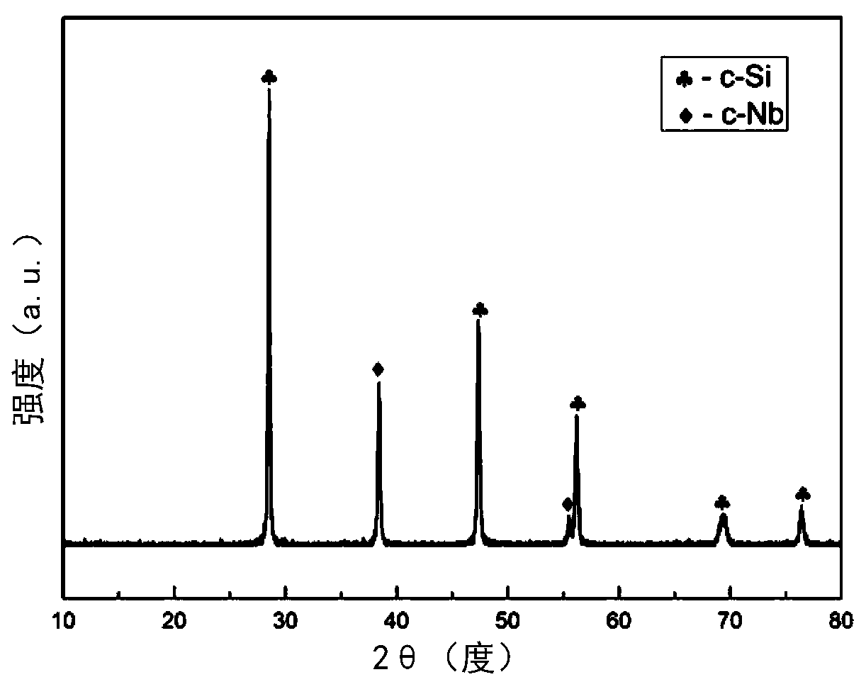
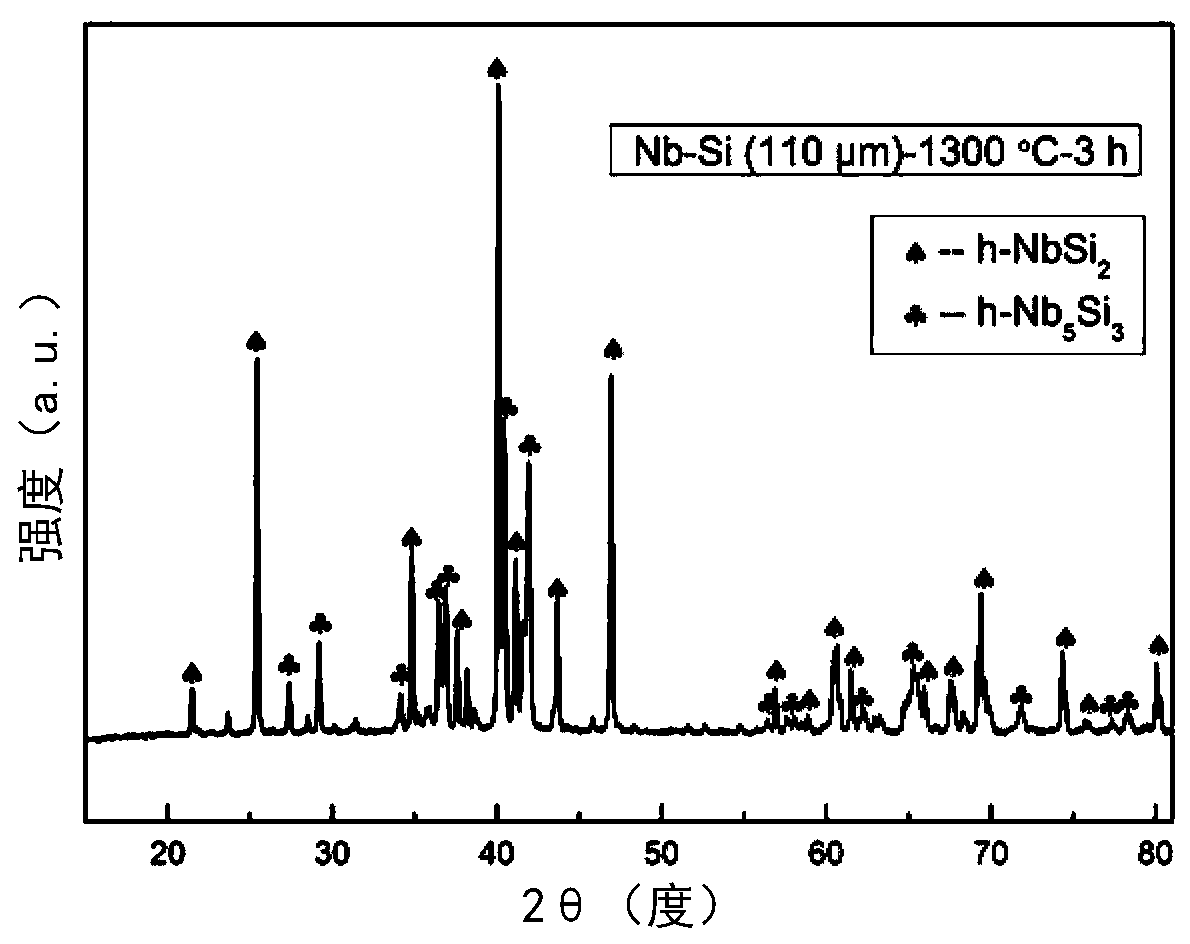
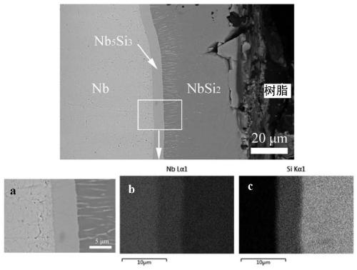
[0035] 3) Using a plasma spraying system (A-2000, Sulzer Metco AG, Switzerland), using the process parameters in Table 2, spraying silicon powder onto the surface of the Nb substrate to form a silicon coating, the thickness of the silicon coating is about 110 μm, figure 1 The XRD results show that the silicon coating is a cubic phase;
[0036] Table 2 is the plasma spraying Si coating process parameters:
[0037]
[0038] 4) Vacuum-atmosphere sintering furnace (ZT-50-2...
PUM
| Property | Measurement | Unit |
|---|---|---|
| particle diameter | aaaaa | aaaaa |
| thickness | aaaaa | aaaaa |
| thickness | aaaaa | aaaaa |
Abstract
Description
Claims
Application Information