
Touch liquid crystal display device avoiding residual images

A technology of liquid crystal display device and liquid crystal display panel, which is applied in the directions of light guide, optics, instruments, etc., can solve the problems of abnormal and unrealistic additional electric field of driving liquid crystal, and achieve the effect of low production cost and simple structure.

Inactive Publication Date: 2018-01-30
星星显示科技(东莞)有限公司
View PDF6 Cites 0 Cited by
  • Summary
  • Abstract
  • Description
  • Claims
  • Application Information

AI Technical Summary

Problems solved by technology

There are many reasons for the afterimage of the liquid crystal display device. One of them is that the driving voltage of the liquid crystal pixel will contain a DC bias voltage component due to the influence of the feed-through voltage or the change of the transistor characteristics, which will cause the abnormality of the additional electric field driving the liquid crystal. resulting in afterimages
Since the afterimage is caused by the nature of the semiconductor itself, it is unrealistic to replace the semiconductor device to improve the afterimage phenomenon caused by this reason

Method used


Image

  • Touch liquid crystal display device avoiding residual images

Examples


Embodiment 1

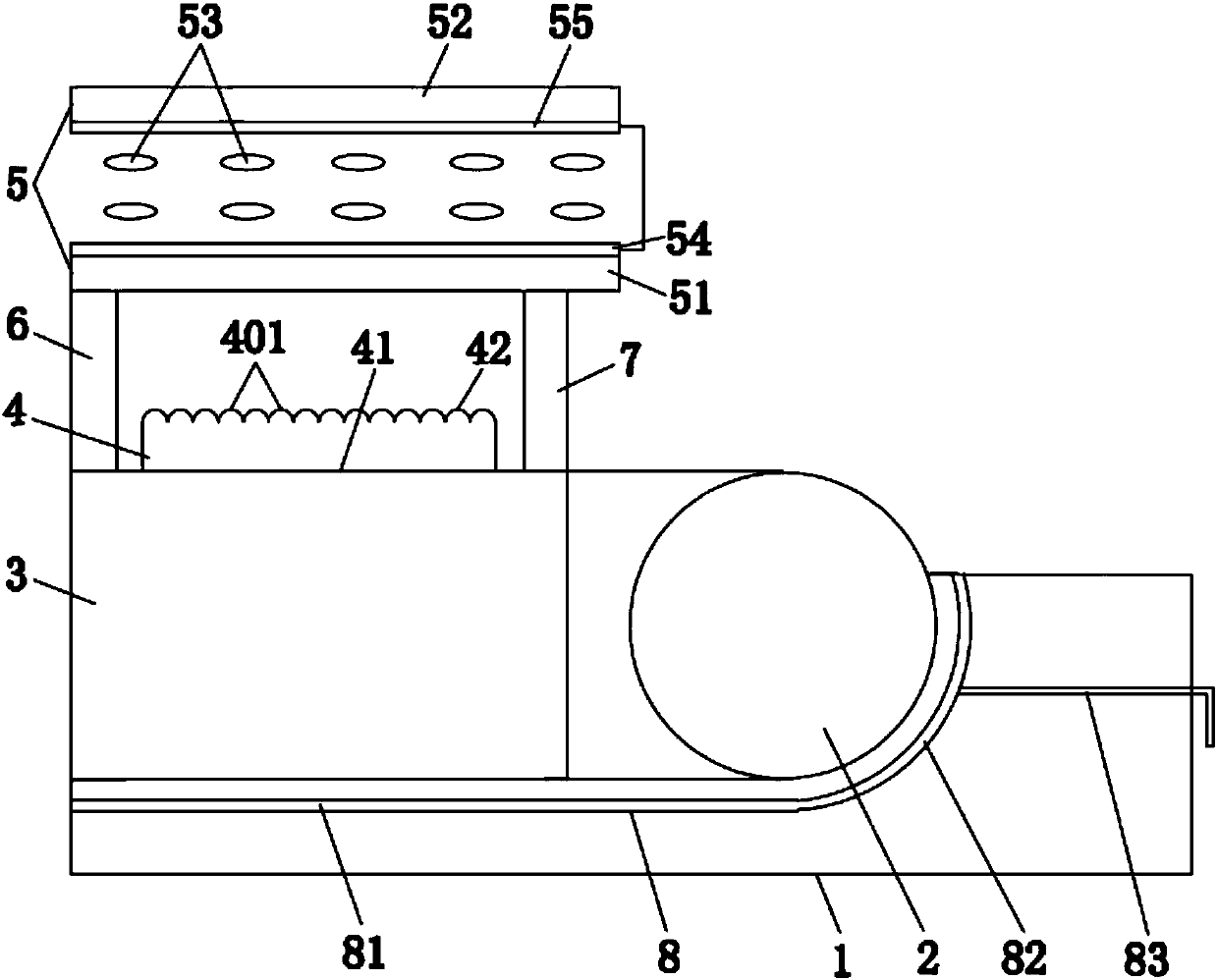
[0033] A touch liquid crystal display device capable of avoiding afterimages in this embodiment, such as figure 1 As shown, it includes a liquid crystal display panel 5 and a backlight module. The liquid crystal display panel 5 includes a first substrate 51 , a second substrate 52 opposite to the first substrate 51 , and a panel between the first substrate 51 and the second substrate 52 . The liquid crystal layer 53; the first substrate 51 is provided with a first liquid metal layer 54 on one side facing the liquid crystal layer 53, and the second liquid metal layer 55 is provided on the side of the second substrate 52 facing the liquid crystal layer 53, and the first liquid metal layer 54 and the liquid crystal layer 53 are provided with The second liquid metal layer 55 is electrically connected; since the first liquid metal layer 54 arranged on the first substrate 51 and the second liquid metal layer 55 arranged on the second substrate 52 are electrically connected to each ot...

Embodiment 2

[0044] Embodiment 2 of a touch liquid crystal display device of the present invention that can avoid afterimages. The difference between this embodiment and Embodiment 1 is that, in this embodiment, the radius of the semicircle 401 is set to 1 mm, and the radius of the semicircle The light-emitting surface 42 spliced ​​by 401 has the characteristics of good light scattering effect, and can avoid light reflection, which can make heat not easy to accumulate, so that the problem of uneven temperature of the entire liquid crystal display device can be further avoided, and the contrast ratio can be improved. , avoid chromatic aberration, and further avoid the occurrence of afterimages. In this embodiment, the diffusion plate 4 is a diffusion plate 4 made of PET plastic, which further has the characteristics of good light scattering effect. Other structures and working principles of this embodiment are the same as those of Embodiment 1, and will not be repeated here.

Embodiment 3

[0046] Embodiment 3 of a touch liquid crystal display device of the present invention that can avoid afterimages. The difference between this embodiment and Embodiment 1 is that in this embodiment, the radius of the semicircle 401 is set to 0.01mm, and the radius of the The light-emitting surface 42 spliced ​​by the semicircles 401 has the characteristics of good light scattering effect, and can avoid light reflection, thereby making it difficult for heat to accumulate, so that the problem of uneven temperature of the entire liquid crystal display device can be further avoided, thereby improving Contrast, avoid chromatic aberration, and further avoid the occurrence of afterimages. In this embodiment, the diffusion plate 4 is a diffusion plate 4 made of HDPE plastic, which further has the characteristics of good light scattering effect. Other structures and working principles of this embodiment are the same as those of Embodiment 1, and will not be repeated here.


PUM

PropertyMeasurementUnit
Radiusaaaaaaaaaa

Abstract

The invention relates to the technical field of liquid crystal display devices, in particular to a touch liquid crystal display device avoiding residual images. The touch liquid crystal display deviceavoiding the residual images comprises a liquid crystal display panel and a backlight module, wherein the liquid crystal display panel comprises a first substrate, a second substrate opposite to thefirst substrate and a liquid crystal layer arranged between the first substrate and the second substrate; a first liquid metal layer is arranged on one face, facing the liquid crystal layer, of the first substrate, a second liquid metal layer is arranged on one face, facing the liquid crystal layer, of the second substrate, and the first liquid metal layer is electrically connected with the secondliquid metal layer; the backlight module comprises a back frame, a backlight source arranged in the back frame and composed of a plurality of light sources in an arranged mode, a light guiding platearranged on one side of the backlight source and a diffusion plate arranged on the light guiding plate; the liquid crystal display panel is arranged on one side of the diffusion plate. By means of thetouch liquid crystal display device, it can be avoided that an additional electric field for driving liquid crystals is abnormal, and occurrence of the residual image phenomenon is thus avoided.

Description

technical field [0001] The invention relates to the technical field of liquid crystal display devices, in particular to a touch-control liquid crystal display device capable of avoiding afterimages. Background technique [0002] The structure of the liquid crystal display device includes a liquid crystal panel and a backlight module. The LCD panel itself does not emit light, and needs the light source provided by the backlight module to display images normally. According to different incidence modes of the light source, the backlight module can be divided into a direct-type backlight module and an edge-type backlight module. Among them, the side-type backlight module is to install the backlight LED strip on the edge of the back panel behind the liquid crystal panel. The light emitted by the LED strip enters the light guide plate from the light incident surface on one side of the light guide plate and is reflected and diffused. It emits from the light-emitting surface of th...

Claims


Application Information

Patent Timeline
IPC IPC(8): G02F1/1333G02F1/13357G02B1/04G02B6/00
Inventor 钟少芬沈广友潘中华
Owner 星星显示科技(东莞)有限公司
Learn More