Flexible ultraviolet (UV) detector of photodetector structure

An ultraviolet detector and phototransistor technology, applied in the field of ultraviolet detectors, can solve the problems of difficulty in realizing miniaturization and arraying of devices, incompatibility of processes, etc., and achieve the effects of strengthening injection and separation, improving detection performance, and high responsivity.

Active Publication Date: 2018-02-16
SOUTHEAST UNIV
View PDF3 Cites 19 Cited by
  • Summary
  • Abstract
  • Description
  • Claims
  • Application Information

AI Technical Summary

Problems solved by technology

For UV detectors based on semiconductors, they usually need to be prepared by means of molecular beam epitaxy on single crystal materials, and the detector target surface technology is not compatible with the single crystal silicon readout integrated circuit (ROIC) process, so they can only Prepared separately, it is difficult to realize the miniaturization and array of devices

Method used


Image

  • Flexible ultraviolet (UV) detector of photodetector structure
  • Flexible ultraviolet (UV) detector of photodetector structure

Examples


Embodiment 1

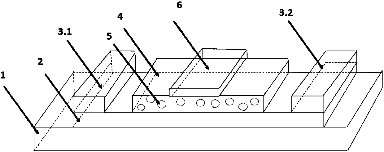
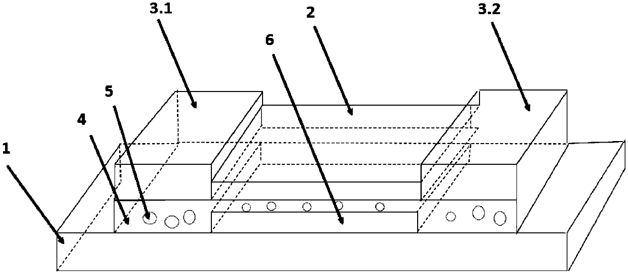
[0031] In the ultraviolet detector of the first inorganic perovskite phototransistor structure of the present invention, the substrate 1 is a glass substrate, and CsPbX is prepared on the substrate 1 3 Thin film 2 serves as the active layer, in CsPbX 3 Preparation of CsPbX with the same substance on the surface of film 2 3 The PMMA organic layer 4 doped with quantum dots 5 is used as the gate insulating layer, which serves as the ultraviolet light sensing window; the source electrode 3.1 and the drain Au electrode 3.2 of the thin film transistor are respectively located on the CsPbX 3 On both sides of the film 2, the FTO gate 6 is located on the CsPbX 3 In the middle of the film 2, under the modulation of the source 3.1 of the thin film transistor, the drain Au electrode 3.2 and the FTO gate 6, the integrated functions of photo-generated carrier separation, converted electrical signal reading, and amplification are obtained to achieve high response Ultraviolet signal detecti...

Embodiment 2

[0038] In the ultraviolet detector of the second inorganic perovskite phototransistor structure of the present invention, the substrate 1 is a glass substrate, an FTO conductive thin film layer is prepared on the substrate 1 as the gate 6, and CsPbX is prepared on the gate 6 3 The PMMA organic layer 4 doped with quantum dots 5 is used as a gate insulating layer, and homogeneous CsPbX is spin-coated on the gate insulating layer 3 Thin film 2 is the active layer, and the source electrode 3.1 and the drain Au electrode 3.2 are located on the CsPbX 3 On both sides of the thin film 2, under the modulation of the source 3.1 of the thin film transistor, the drain Au electrode 3.2 and the FTO gate 6, the integrated functions of photo-generated carrier separation, converted electrical signal reading, and amplification are obtained to achieve high-responsiveness UV signal detection. CaB 3 Quantum dots are synthesized and purified in the same way as in Example 1.

[0039] The phototra...

Embodiment 3

[0045] CaB 3 Quantum dots are synthesized and purified in the same way as in Example 1.

[0046] The fabrication process of the flexible phototransistor is as follows:

[0047] a) Preparation of FTO grid 6: On the PET substrate 1, a magnetron sputtering technique is used to prepare an FTO transparent film, and a photolithography technique is used to prepare an FTO gate electrode.

[0048] b) Preparation of gate insulating layer 4: CsPbX 3 The molar ratio of quantum dots and PMMA is dissolved in toluene solution with a concentration of 20 mg / mL. The film is formed by spin coating on the surface of the substrate on which the FTO gate has been formed. A gate insulating layer with uniform photoresponse characteristics.

[0049] c) Prepare the channel layer: prepare CsPbX on the gate insulating layer by spin coating 3 Film 2, spin coating speed 2000rpm, time 30s, CsPbX 3 Quantum dot concentration 20mg / mL, annealed at 130°C for 15min.

[0050] d) The process for preparing the ...


PUM


Abstract

The invention relates to and provides an ultraviolet (UV) detector of an inorganic perovskite phototransistor structure. A substrate (1) is a glass substrate, a CsPbX3 thin film (2) is prepared on thesubstrate (1) as an active layer, a PMMA organic layer (4) doped with CsPbX3 quantum dots (5) is prepared by the same material on the surface of the CsPbX3 thin film (2) as a gate insulating layer, and the CsPbX3 quantum dots are taken as a UV light sensing window; a source electrode (3.1) and a drain Au electrode (3.2) of the thin film transistor are respectively located on two sides of the CsPbX3 thin film (2), an FTO gate electrode (6) is located in the middle on the CsPbX3 thin film (2), and the integrated function of photo-generated carrier separation, converted electrical signal readingand amplification is obtained under the modulation of the source electrode (3.1), the drain Au electrode (3.2) and the FTO gate (6) of the thin film transistor, so as to achieve high response UV signal detection. The phototransistor detector can adopt a top-gate structure as shown in FIG.1 or a bottom-gate structure as shown in FIG.2. The above two structures can be prepared on the glass substrate and also be prepared on a flexible substrate to form the flexible phototransistor UV detector of the bottom-gate or top-gate structure.

Description

technical field [0001] The invention relates to a novel ultraviolet detector technology with a phototransistor structure, which belongs to the field of photoelectric detection technology. Background technique [0002] Ultraviolet photodetectors and related technologies are widely used in military and civilian applications, such as missile early warning and tracking, ultraviolet light communication, engine work monitoring, deep space exploration research, ultraviolet astronomy, environmental monitoring, fire detection and alarm, and medicine. detection and so on. Therefore, ultraviolet detection technology has always been an international research hotspot and one of the main technical fields of competition in various countries. [0003] With the development of information technology, while improving performance, there is an urgent need for ultraviolet detection devices to develop in the direction of miniaturization, arrayization and flexibility. For UV detectors based on se...

Claims


Application Information

Patent Timeline
Patent Type & Authority Applications(China)
IPC IPC(8): H01L31/101H01L31/112H01L31/18
CPCH01L31/101H01L31/112H01L31/18Y02P70/50
Inventor 李青雷威张镇波孙义张旭
Owner SOUTHEAST UNIV
Why Eureka
Try Eureka