A kind of preparation method of gallium nitride epitaxial structure based on hexagonal boron nitride-graphene composite layer as buffer layer

A technology of graphene composite and hexagonal boron nitride, which is applied in the field of optoelectronics, can solve problems such as difficult to control growth conditions, and achieve good thickness controllability, easy operation, and stress reduction effects

Active Publication Date: 2020-03-20
INST OF ELECTRONICS ENG CHINA ACAD OF ENG PHYSICS
View PDF5 Cites 0 Cited by
  • Summary
  • Abstract
  • Description
  • Claims
  • Application Information

AI Technical Summary

Problems solved by technology

This technical solution requires multiple growths, and it is not easy to control the growth conditions when growing two or more two-dimensional derivative films

Method used


Image

  • A kind of preparation method of gallium nitride epitaxial structure based on hexagonal boron nitride-graphene composite layer as buffer layer
  • A kind of preparation method of gallium nitride epitaxial structure based on hexagonal boron nitride-graphene composite layer as buffer layer
  • A kind of preparation method of gallium nitride epitaxial structure based on hexagonal boron nitride-graphene composite layer as buffer layer

Examples


Embodiment 1

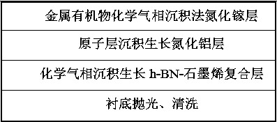
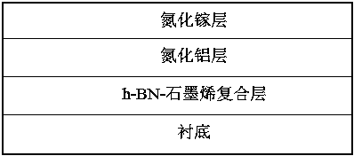
[0039] A method for preparing a gallium nitride epitaxial structure based on a hexagonal boron nitride-graphene composite layer as a buffer layer, comprising the following process steps:

[0040] A, polishing and cleaning the copper substrate;

[0041] B, grow h-BN-graphene composite layer on copper substrate;

[0042]C, utilize atomic layer deposition to grow a layer of aluminum nitride layer on the h-BN-graphene composite layer;

[0043] D. A gallium nitride layer is grown on the thin aluminum nitride layer by metal-organic chemical vapor deposition.

Embodiment 2

[0045] A method for preparing a gallium nitride epitaxial structure based on a hexagonal boron nitride-graphene composite layer as a buffer layer, comprising the following process steps:

[0046] A, polishing and cleaning the copper substrate;

[0047] B, grow h-BN-graphene composite layer on copper substrate;

[0048] C, utilize atomic layer deposition to grow a layer of aluminum nitride layer on the h-BN-graphene composite layer;

[0049] D. A gallium nitride layer is grown on the thin aluminum nitride layer by metal-organic chemical vapor deposition.

[0050] In step A, specifically:

[0051] Firstly, the copper substrate was cleaned to remove the oil and oxide layer on the surface, and then after double polishing by mechanical polishing and electrochemical polishing, it was washed three times with ethanol and deionized water in turn, washed with dilute hydrochloric acid for 5 minutes, cleaned with deionized water, and blown with nitrogen. Dry to obtain a copper substrat...

Embodiment 3

[0053] A method for preparing a gallium nitride epitaxial structure based on a hexagonal boron nitride-graphene composite layer as a buffer layer, comprising the following process steps:

[0054] A, polishing and cleaning the copper substrate;

[0055] B, grow h-BN-graphene composite layer on copper substrate;

[0056] C, utilize atomic layer deposition to grow a layer of aluminum nitride layer on the h-BN-graphene composite layer;

[0057] D. A gallium nitride layer is grown on the thin aluminum nitride layer by metal-organic chemical vapor deposition.

[0058] In step A, specifically:

[0059] Firstly, the copper substrate was cleaned to remove the oil stain and oxide layer on the surface, and after the double polishing of mechanical polishing and electrochemical polishing, it was washed three times with ethanol and deionized water in turn, washed with dilute hydrochloric acid for 10 minutes, washed with deionized water, and blown with nitrogen. Dry to obtain a copper sub...


PUM

PropertyMeasurementUnit
thicknessaaaaaaaaaa
thicknessaaaaaaaaaa
lattice constantaaaaaaaaaa

Abstract

The invention relates to a preparation method of a GaN epitaxial structure taking a hexagonal BN-graphene composite layer as a buffer layer, and belongs to the technical field of photoelectron. The method comprises the steps of polishing and cleaning a copper substrate; growing an h-BN-graphene composite layer on the copper substrate; growing an AlN layer on the h-BN-graphene composite layer by anatomic layer deposition method; and growing a GaN layer on the AIN thin layer by a metal organic matter chemical vapor deposition method. The h-BN-graphene composite layer is used as the buffer layerbetween the copper substrate and the GaN epitaxial layer, thus, the problems of defect dislocation, crack and the like caused by lattice mismatching and thermal mismatching between the substrate andthe epitaxial layer can be solved, the stress between the substrate and an epitaxial material is effectively reduced, and the quality of the GaN epitaxial layer is improved.

Description

technical field [0001] The invention relates to a method for preparing a gallium nitride epitaxial structure, more specifically, the invention relates to a method for preparing a gallium nitride epitaxial structure based on a hexagonal boron nitride-graphene composite layer as a buffer layer, which belongs to optoelectronic technology field. Background technique [0002] GaN material has received more and more attention as a new type of semiconductor material. As a representative material of the third-generation semiconductor, gallium nitride has excellent electrical and optical properties. It has the advantages of wide bandgap, direct bandgap, high temperature and high pressure resistance, and high electron mobility. It is used in the fields of electronic devices and optoelectronic devices. It has a wide range of applications, so the preparation of high-quality gallium nitride is the key to the preparation of the above devices. [0003] Graphene is a new type of two-dimen...

Claims


Application Information

Patent Timeline
Patent Type & Authority Patents(China)
IPC IPC(8): H01L33/12H01L33/00
CPCH01L33/005H01L33/12
Inventor 王文杰李沫李俊泽张建杨浩军谢武泽邓泽佳代刚张健
Owner INST OF ELECTRONICS ENG CHINA ACAD OF ENG PHYSICS
Why Eureka
Try Eureka