Cold cathode structure based on graphene oxide/graphene micro emission area and preparation method thereof

An emission area and graphene technology, which is applied in cold cathode manufacturing, discharge tube/lamp manufacturing, electrode system manufacturing, etc., can solve the problem of inability to better realize the development and application of fine and fine display technology, the emission current cannot be controlled, and the Issues such as realizing different field emission

Active Publication Date: 2018-02-23
XI'AN PETROLEUM UNIVERSITY
View PDF3 Cites 2 Cited by
  • Summary
  • Abstract
  • Description
  • Claims
  • Application Information

AI Technical Summary

Problems solved by technology

Although these research works can increase the emission current and improve the stability of field emission macroscopically as a whole, they cannot control the emission current on the micro-region at the top of the emitter, nor can they realize different field emissions in the micro-region at the top of the same emitter. Unable to better realize the development and application of fine and fine display technology

Method used


Image

  • Cold cathode structure based on graphene oxide/graphene micro emission area and preparation method thereof
  • Cold cathode structure based on graphene oxide/graphene micro emission area and preparation method thereof
  • Cold cathode structure based on graphene oxide/graphene micro emission area and preparation method thereof

Examples


Embodiment Construction

[0036] The present invention will be further described in detail below in conjunction with specific embodiments, which are explanations of the present invention rather than limitations.

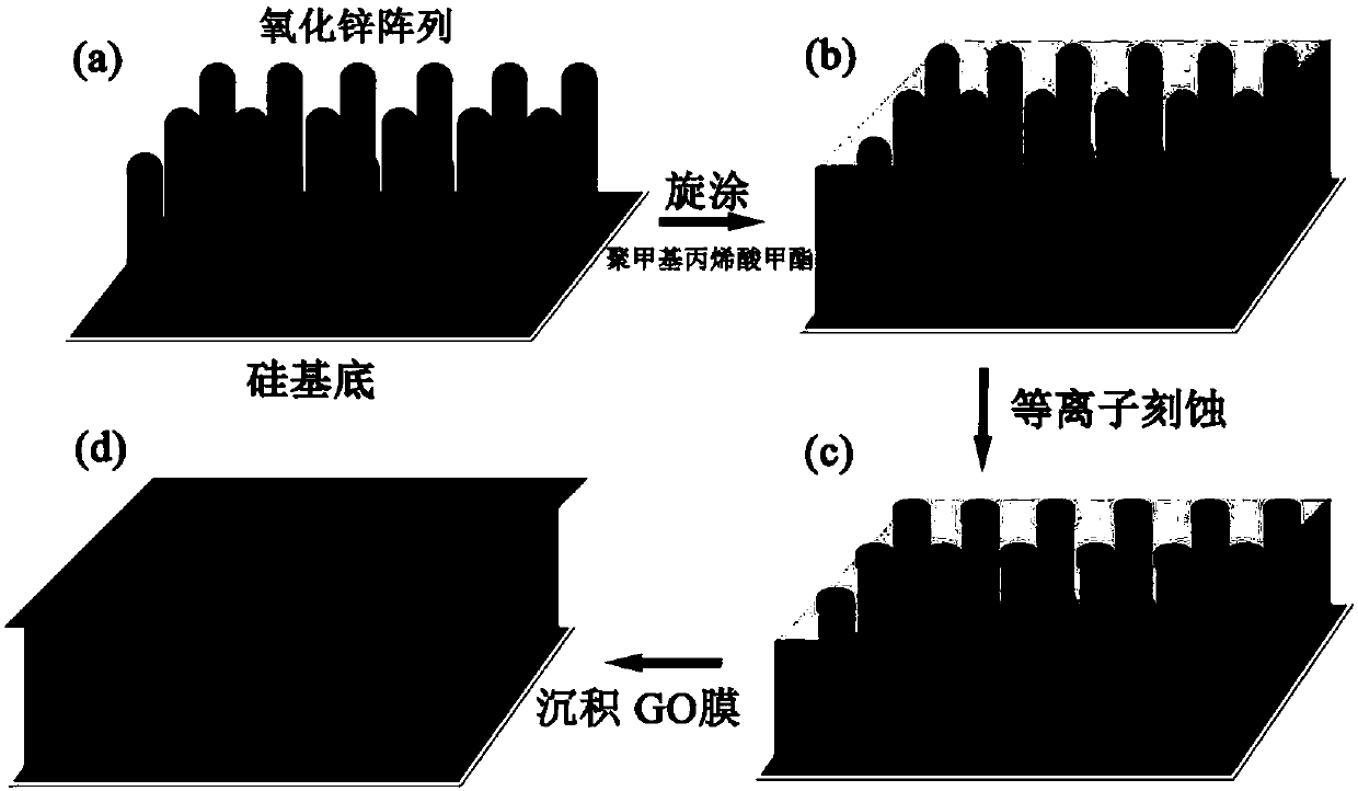
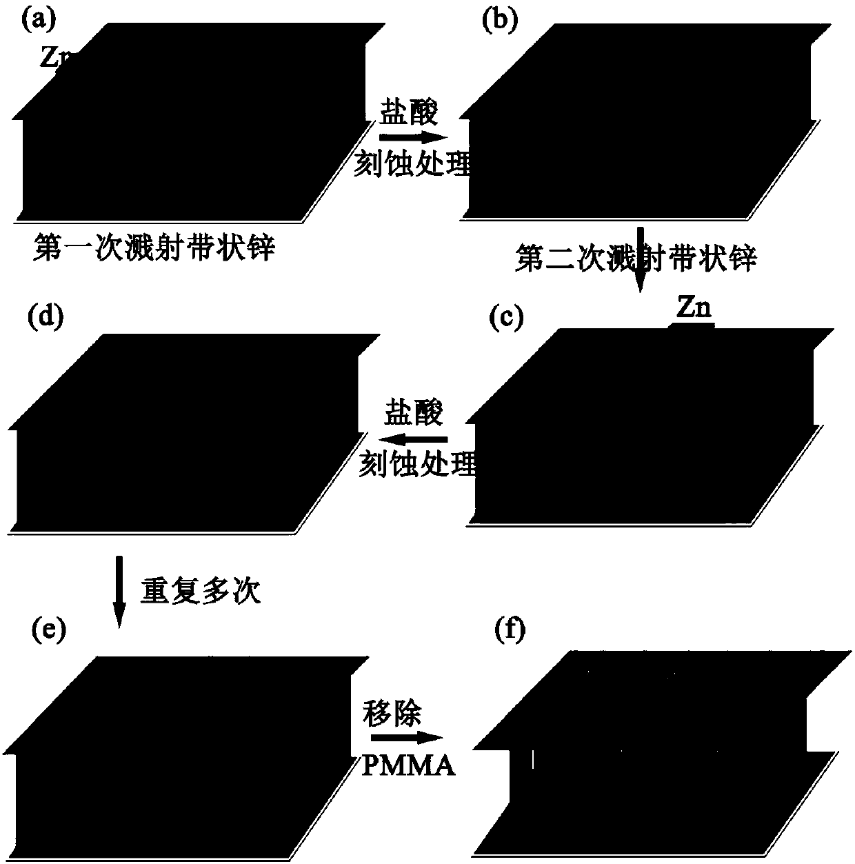
[0037] In the present invention, GO is evenly coated on the top of the PMMA-ZnO nano-array, combined with mask photolithography and magnetron sputtering methods, the surface of the GO layer on the top of the PMMA-ZnO nano-array is formed by GO and various layers and different reductions. The micro-emitting regions composed of graphene interphases, that is, the GO / G-PMMA-ZnO structure, can study the dependence of the electron emission density and intensity in different micro-regions on the preparation parameters, and optimize the micro-regions, further Improve its field emission performance and provide reliable experimental parameters and theoretical basis for future assembly of high-resolution fine display devices.

[0038] Since graphene is one of the low-Z materials with the lowest backscat...


PUM

PropertyMeasurementUnit
thicknessaaaaaaaaaa
thicknessaaaaaaaaaa
widthaaaaaaaaaa

Abstract

The invention provides a cold cathode structure based on a graphene oxide / graphene micro emission area and a preparation method thereof. The cold cathode structure comprises a silicon substrate, a ZnOnano-array which is vertically arranged and grows on the silicon substrate, and a surface emission layer coated on the top of the ZnO nano-array. The surface emission layer is composed of graphene oxide blocks and graphene blocks, wherein the graphene oxide blocks and the graphene blocks are integrally arranged. The graphene oxide blocks are arranged horizontally and longitudinally at intervals,and the remaining areas are filled with the graphene blocks. The graphene oxide blocks and graphene blocks with different thicknesses and degrees of reduction form the micro emission area. The methodcomprises the steps that an electrophoretic deposition technology is used to prepare a GO layer on the top of the one-dimensional ZnO nano-array; GO is reverted to graphene by using magnetron sputtering zinc oxide; the graphene layer is thinned by using hydrochloric acid to etch zinc; and the GO / G alternated micro region is acquired on the top of the ZnO nano-array through multiple mask sputteringand etching.

Description

technical field [0001] The invention relates to a cold cathode field emission material, in particular to a graphene oxide / graphene-based cold cathode micro emission region and a preparation method thereof. Background technique [0002] Finding cold cathode field emission materials with excellent performance is the goal that researchers have been pursuing. It has been reported that the materials with high field emission current density and stability can be obtained by synthesizing new materials or modifying existing materials. Good and good emitter material such as the tip is not easy to burn out. Although these research works can increase the emission current and improve the stability of field emission macroscopically as a whole, they cannot control the emission current on the micro-region at the top of the emitter, nor can they realize different field emissions in the micro-region at the top of the same emitter. It is impossible to better realize the development and applic...

Claims


Application Information

Patent Timeline
Patent Type & Authority Applications(China)
IPC IPC(8): H01J1/304H01J9/02B82Y30/00B82Y40/00
CPCB82Y30/00B82Y40/00H01J1/3044H01J9/025
Inventor 丁继军陈海霞冯德全傅海威
Owner XI'AN PETROLEUM UNIVERSITY
Why Eureka
Try Eureka