Preparation method of AlGaInP thin film LED chip dicing line

A technology of LED chips and dicing lanes, which is applied in semiconductor/solid-state device manufacturing, electrical components, circuits, etc., can solve the problems of highly toxic elemental bromine, hidden dangers to the health of craftsmen and environmental safety, and difficulty in controlling the stability and consistency of corrosive liquids and other issues, to achieve good stability and consistency, and to protect the health of the body and the environment

Inactive Publication Date: 2018-02-23
NANCHANG UNIV +1
View PDF4 Cites 2 Cited by
  • Summary
  • Abstract
  • Description
  • Claims
  • Application Information

AI Technical Summary

Problems solved by technology

The stability and consistency of the corrosive solution are difficult to control, and the elemental bromine u

Method used


Image

  • Preparation method of AlGaInP thin film LED chip dicing line
  • Preparation method of AlGaInP thin film LED chip dicing line
  • Preparation method of AlGaInP thin film LED chip dicing line

Examples


Embodiment 1

[0028] A method for preparing AlGaInP thin film LED chip dicing lines, comprising the following steps:

[0029] First, the epitaxial material is prepared by conventional MOCVD, and then the epitaxial material is transferred to the bonded substrate by using metal evaporation, photolithography, corrosion, bonding, and alloying.

[0030] At this time, the AlGaInP thin film LED chips are connected. In order to divide the AlGaInP thin film LED chips, it is necessary to prepare a dicing line, and then perform AlGaInP thin film LED chip point measurement and AlGaInP thin film LED chip cutting. The specific steps are as follows:

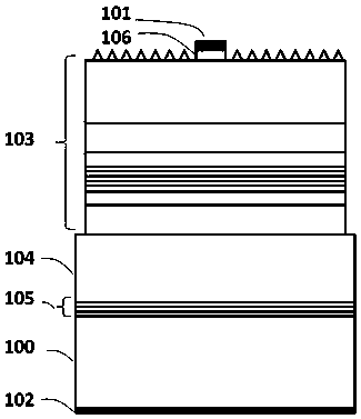
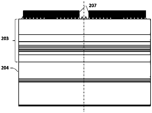
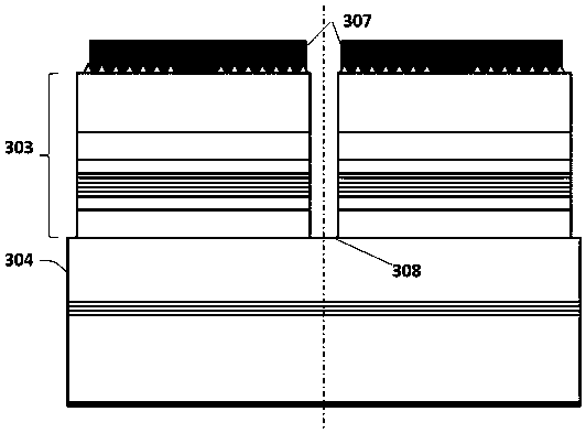
[0031] A. Coat the photoresist on the surface of the AlGaInP thin film LED chip, remove the photoresist in the area corresponding to the cutting line of the AlGaInP thin film LED chip by conventional photolithography process, and expose the AlGaInP LED epitaxial material. At this time, the structure is as follows figure 2 shown;

[0032] B. Preparation of ...

Embodiment 2

[0040] A method for preparing AlGaInP thin film LED chip dicing lines, comprising the following steps:

[0041] First, the epitaxial material is prepared by conventional MOCVD, and then the epitaxial material is transferred to the bonded substrate by using metal evaporation, photolithography, corrosion, bonding, and alloying.

[0042] At this time, the AlGaInP thin film LED chips are connected. In order to divide the AlGaInP thin film LED chips, it is necessary to prepare a dicing line, and then perform AlGaInP thin film LED chip point measurement and AlGaInP thin film LED chip cutting. The specific steps are as follows:

[0043] A. Coat the photoresist on the surface of the AlGaInP thin film LED chip, remove the photoresist in the area corresponding to the cutting line of the AlGaInP thin film LED chip by conventional photolithography process, and expose the AlGaInP LED epitaxial material. At this time, the structure is as follows figure 2 shown;

[0044] B. Preparation of ...

Embodiment 3

[0052] A method for preparing AlGaInP thin film LED chip dicing lines, comprising the following steps:

[0053] First, the epitaxial material is prepared by conventional MOCVD, and then the epitaxial material is transferred to the bonded substrate by using metal evaporation, photolithography, corrosion, bonding, and alloying.

[0054] At this time, the AlGaInP thin film LED chips are connected. In order to divide the AlGaInP thin film LED chips, it is necessary to prepare a dicing line, and then perform AlGaInP thin film LED chip point measurement and AlGaInP thin film LED chip cutting. The specific steps are as follows:

[0055] A. Coat the photoresist on the surface of the AlGaInP thin film LED chip, remove the photoresist in the area corresponding to the cutting line of the AlGaInP thin film LED chip by conventional photolithography process, and expose the AlGaInP LED epitaxial material. At this time, the structure is as follows figure 2 shown;

[0056] B. Preparation of ...


PUM


Abstract

The invention discloses a preparation method of an AlGaInP thin film LED chip dicing line. The method comprises the steps that an AlGaInP LED epitaxial material is prepared by a conventional MOCVD, and then the epitaxial material is transferred onto a bond substrate by using conventional die preparation processes such as metal evaporation, photoetching, corroding, bonding and alloying to prepare the AlGaInP thin film LED chip with N light-emitting sides; before the AlGaInP thin film LED chip is cut and separated, a photoetching process is used to protect the area other than a dicing line witha photoresist; the AlGaInP thin film LED chip to be cut is put into a dicing line corrosive liquid prepared from aqueous solution of iodic acid, hydrochloric acid and water to corrode the epitaxial material in the corresponding area of the dicing line to prepare the dicing line; and finally, a laser dicing machine or an abrasive wheel dicing machine is used to separate the AlGaInP thin film LED chip along the centerline of the dicing line. According to the invention, the method has good stability and consistency; and the dicing line corrosive liquid is free of highly toxic elemental bromine, which is beneficial to the health of craftsmen and environmental protection.

Description

technical field [0001] The invention relates to the field of semiconductor light emitting devices, in particular to a method for preparing AlGaInP thin film LED chip dicing lines. Background technique [0002] Semiconductor light-emitting diodes (Light-Emitting Diodes, LEDs) have been widely used in many fields, and are recognized as the next generation of green lighting sources. The AlGaInP material lattice-matched with gallium arsenide substrates can cover visible light wavelengths from 560nm to 650nm, and is an excellent material for preparing deep red, red, orange, and yellow-green LEDs. [0003] AlGaInP light-emitting diodes have important applications in solid-state lighting, display, urban lighting, plant growth and other fields, and are widely used in full-color screen displays, car lights, traffic lights, stage floodlights, plant growth lights and high color rendering index White light lighting and other products. [0004] In recent years, people have made great p...

Claims


Application Information

Patent Timeline
IPC IPC(8): H01L21/304H01L21/306H01L21/308H01L33/00
CPCH01L21/3043H01L21/30612H01L21/308H01L33/0075H01L33/0093
Inventor 李树强陈芳施维王光绪江风益
Owner NANCHANG UNIV
Why Eureka
Try Eureka