Longitudinal-BJT-triggered SCR device used for ESD protection

A device and vertical technology, applied in the field of SCR devices triggered by vertical BJT and horizontal silicon controlled rectifier SCR, can solve the problems of lowering the upper limit of ESD design window and shrinking feature size

Active Publication Date: 2018-02-23
UNIV OF ELECTRONICS SCI & TECH OF CHINA
View PDF4 Cites 13 Cited by
  • Summary
  • Abstract
  • Description
  • Claims
  • Application Information

AI Technical Summary

Problems solved by technology

[0006] With the continuous advancement of integrated circuit technology, the feature size continues to shrink; the continuous thinning of the MOSFET gate oxide layer makes the breakdown voltage BVox of the gate oxide layer continue to decrease, which greatly reduces the upper limit o...

Method used


Image

  • Longitudinal-BJT-triggered SCR device used for ESD protection
  • Longitudinal-BJT-triggered SCR device used for ESD protection
  • Longitudinal-BJT-triggered SCR device used for ESD protection

Examples


Embodiment 1

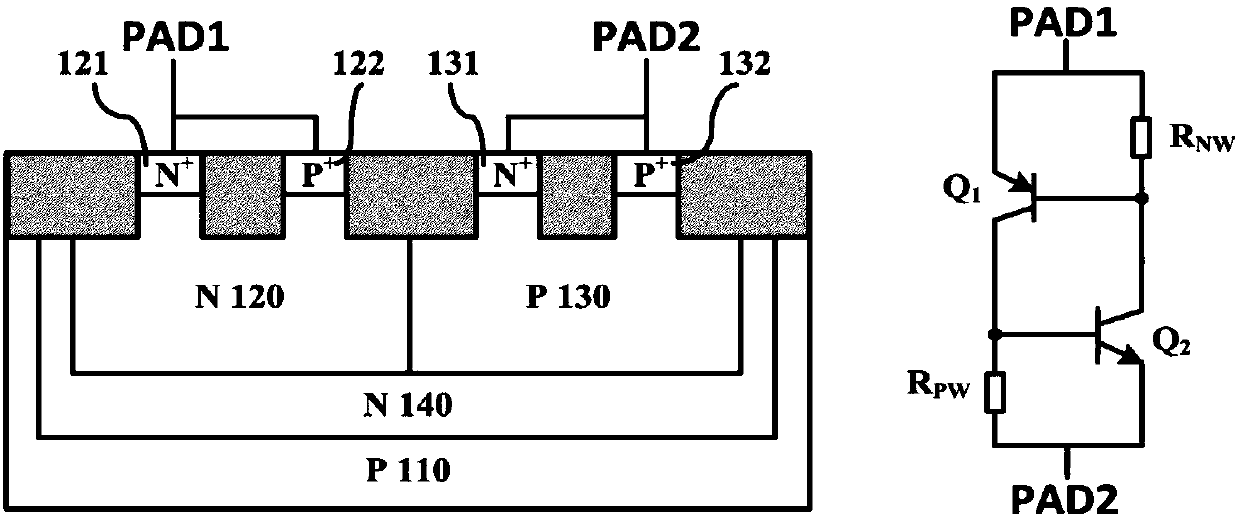
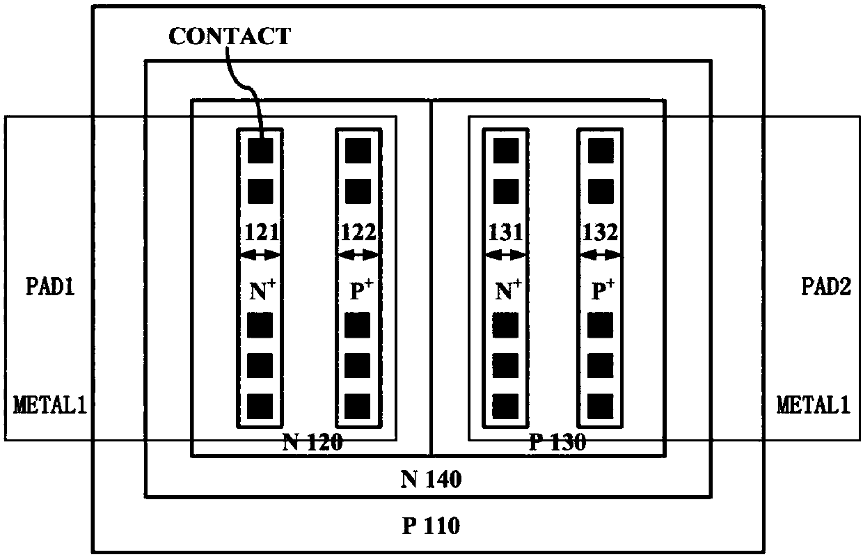
[0024] This embodiment provides an SCR device triggered by a vertical BJT for ESD protection, its structure is as follows Figure 4 As shown, the left figure is a schematic diagram of the structure, and the right figure is an equivalent circuit diagram of the structure; a layout implementation method is as follows Figure 5 shown. The structure of the SCR device (VBTSCR_type1) triggered by the vertical BJT includes a p-type silicon substrate 110; an n-type deep well 140 is formed on the substrate, and its function is to isolate the SCR device above it from the p-type silicon substrate A well region is formed on the n-type deep well 140, and the well region includes an n-type well region 120 and a p-type well region 130, and the two well regions are adjacent; wherein, in the n-type well region 120 From left to right, a first n-type heavily doped region 122, a second n-type heavily doped region 123, a first p-type heavily doped region 124, and a p-type moderately doped region 1...

Embodiment 2

[0026] This embodiment provides an SCR device triggered by a vertical BJT for ESD protection, its structure is as follows Figure 6 As shown, the left figure is a schematic diagram of the structure, and the right figure is an equivalent circuit diagram of the structure; a layout implementation method is as follows Figure 7 shown. The structure of the SCR device (VBTSCR_type2) triggered by the vertical BJT includes a p-type silicon substrate 110; an n-type deep well 140 is formed on the substrate, and its function is to isolate the SCR device above it from the p-type silicon substrate A well region is formed on the n-type deep well 140, and the well region includes an n-type well region 120 and a p-type well region 130, and the two well regions are adjacent; wherein, in the n-type well region 120 From left to right, there are a second n-type heavily doped region 123, a first p-type heavily doped region 124, a first n-type heavily doped region 122, and a p-type moderately dope...


PUM


Abstract

The invention belongs to the field of electronic technologies, and particularly provides a longitudinal-BJT-triggered SCR device used for ESD protection. The longitudinal-BJT-triggered SCR device (VBTSCR) introduces an extra triggering path on the basis of a traditional LSCR device. An ESD injection layer is introduced into a first conduction type well region, so as to form a longitudinal-structure base region floating NPN transistor. The ESD injection layer is a P-type doped region with a medium doping concentration, and the doping concentration thereof is between a drain/source heavily-dopedactive region concentration and a well region doping concentration. According to the SCR device, a common-emitter collector junction avalanche breakdown voltage BV<CEO> of the longitudinal-structurebase region floating NPN transistor is very low, when the base region floating NPN transistor serves as a triggering device of the SCR, significant reduction of the triggering voltage of the SCR device can be realized, thereby realizing the effect of providing effective ESD protection for circuits in an advanced nanometer technology.

Description

technical field [0001] The invention belongs to the field of electronic technology, and in particular relates to the design of an electrostatic discharge (ESD: Electro-Static discharge) protection circuit, especially a lateral silicon-controlled rectifier SCR (Silicon-Controlled-Rectifier referred to as SCR), specifically a device for ESD protection relies on vertical BJT triggered SCR devices. Background technique [0002] Electro-Static Discharge (ESD) is an event in which a limited charge is transferred between two objects of different potentials. In people's daily life, ESD phenomena can be seen everywhere; for example, at a relative humidity of 10%, people walking on carpets can generate up to 35,000 volts of electrostatic voltage. For integrated circuits, from production to transportation, system integration and user use, all processes may generate electrostatic discharge on the pins of integrated circuits. The instantaneous high-voltage electrostatic pulse generated...

Claims


Application Information

Patent Timeline
IPC IPC(8): H01L27/02
CPCH01L27/0262H01L27/0292
Inventor 杜飞波刘继芝刘志伟
Owner UNIV OF ELECTRONICS SCI & TECH OF CHINA
Why Eureka
Try Eureka