Novel microwave three-dimensional integrated system-in-package interconnection structure

A system-level packaging and interconnection structure technology, applied in the field of microwave three-dimensional integrated system-level packaging and interconnection structures, to achieve the effect of reducing interconnection size, high processing accuracy, and maintaining signal integrity

Active Publication Date: 2018-02-27
NO 55 INST CHINA ELECTRONIC SCI & TECHNOLOGYGROUP CO LTD
View PDF4 Cites 7 Cited by
  • Summary
  • Abstract
  • Description
  • Claims
  • Application Information

AI Technical Summary

Problems solved by technology

[0004] However, the realization of 3D integrated system-in-package interconnection of GaAs chips based on traditional technology has not been reported; therefore, it is necessary to further design a new microwave 3D integrated system-in-package interconnection technology in order to realize the existing commercial GaAs chips in Application and extension in SoP

Method used


Image

  • Novel microwave three-dimensional integrated system-in-package interconnection structure
  • Novel microwave three-dimensional integrated system-in-package interconnection structure

Examples


Embodiment 1

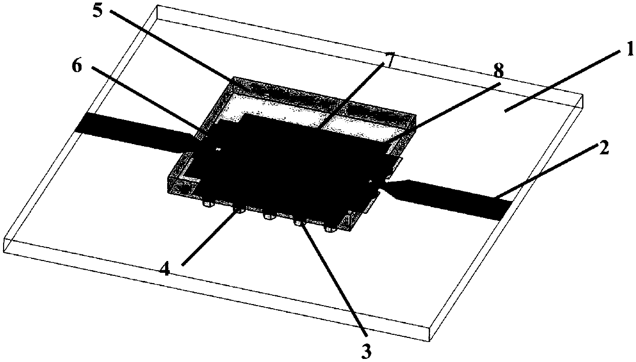
[0020] Such as figure 1 As shown, a microwave three-dimensional integrated system-in-package interconnection structure includes a substrate dielectric substrate 1, a microstrip line 2 on the substrate dielectric substrate, a ground metallization hole array 3 on the substrate dielectric substrate, a gallium arsenide chip 4, Silicon substrate 5, coplanar waveguide transmission line 6 on the silicon substrate, buried cavity 7 opened in the silicon substrate above the sensitive position of the gallium arsenide chip, metallized hole array ground plane metal 8 on the upper surface of the substrate medium; the sensitive position refers to part of the interior lines or active areas.

[0021] The gallium arsenide chip 4 is arranged between the silicon substrate 5 and the ground plane metal 8 , the buried cavity 7 is not penetrated above, and the microstrip line 2 is connected to the gallium arsenide chip 4 through a coplanar waveguide transmission line 6 .

Embodiment 2

[0023] The difference between this embodiment and Embodiment 1 is that a penetrating non-metallized groove is opened above the sensitive position of the gallium arsenide chip.

Embodiment 3

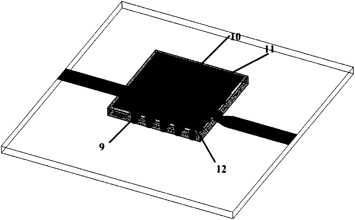
[0025] Such as figure 2 As shown, the difference between this embodiment and Embodiment 1 is that the interconnection structure also includes solder balls 10, through-silicon vias 11 for grounding the microstrip transmission line in the silicon substrate, and a reference ground plane 12 for the microstrip transmission line on the top surface of the silicon substrate. , the solder balls 10 are used to connect the silicon substrate 5 and the ground plane metal 8 .

[0026] The gallium arsenide chip 4 is interconnected with the microstrip transmission line 9 on the silicon substrate through flip-chip, and then the entire vertical interconnection structure is flipped onto the substrate dielectric substrate through solder balls 10, and passes through the microstrip line 2 on the substrate dielectric substrate. Interconnect with other components of the system.

[0027] The manufacturing process is as follows: flip-chip the gallium arsenide chip 4 onto the silicon substrate 5, and ...


PUM


Abstract

The invention discloses a novel microwave three-dimensional integrated system-in-package interconnection structure. The microwave three-dimensional integrated system-in-package interconnection structure comprises a substratum medium substrate, a microstrip line, a grounded metallization hole array, a millimeter wave monolithic integrated circuit and a silicon substrate, and the grounded metallization hole array, the millimeter wave monolithic integrated circuit and the silicon substrate are arranged on substratum medium substrate; grounded planar metal is arranged on the grounded metallizationhole array, and the millimeter wave monolithic integrated circuit is arranged between a silicon substrate and grounded planar metal; a cavity is formed in the silicon substrate above a sensitive position of the millimeter wave monolithic integrated circuit; the microstrip line is connected with the millimeter wave monolithic integrated circuit through a planar transmission line. Compared with traditional golden wire bonding, the interconnection size among chips is obviously reduced, which is beneficial to maintenance of signal integrity during transmission of radio frequency and high-speed digital signals.

Description

technical field [0001] The invention belongs to the technical field of electromagnetic fields and microwaves, and in particular relates to a novel microwave three-dimensional integrated system-level packaging and interconnection structure. Background technique [0002] With the continuous development of electronic information systems towards miniaturization, high performance, and multi-function, System on Package (SoP) provides a miniaturized integration solution for electronic information systems. SoP has been used in computers, mobile phones, Sensors, vehicle radar and other military and civilian fields have been widely researched and applied. However, most of the interconnections involving radio frequency chips in the current SoP are completed by gold wire bonding. The existence of gold wire is not conducive to the further integration and miniaturization of the entire system, and the gold wire interconnection at high frequency affects the work of the chip. Performance, t...

Claims


Application Information

Patent Timeline
Patent Type & Authority Applications(China)
IPC IPC(8): H01L23/488H01P3/08
CPCH01L23/488H01P3/081
Inventor 张君直施永荣
Owner NO 55 INST CHINA ELECTRONIC SCI & TECHNOLOGYGROUP CO LTD
Why Eureka
Try Eureka