Method for preparing A-phase vanadium dioxide film through magnetron sputtering
A technology of vanadium dioxide and magnetron sputtering, which is applied in sputtering coating, metal material coating process, vacuum evaporation coating, etc., to achieve the effect of easy control and simple operation
- Summary
- Abstract
- Description
- Claims
- Application Information
AI Technical Summary
Problems solved by technology
Method used
Image
Examples
Embodiment 1
[0025] Vanadium dioxide ceramic target is used, the sputtering gas is argon with a purity of 99.99%, the reaction gas is oxygen with a purity of 99.99%, and the background vacuum is controlled to be 1×10 -4 Pa, deposition temperature 450°C, deposition total pressure 3.0Pa, oxygen partial pressure 1%, sputtering power 100W, sputter vanadium dioxide thin film on (110) surface strontium titanate substrate for 70 minutes. Cool down naturally after sputtering.
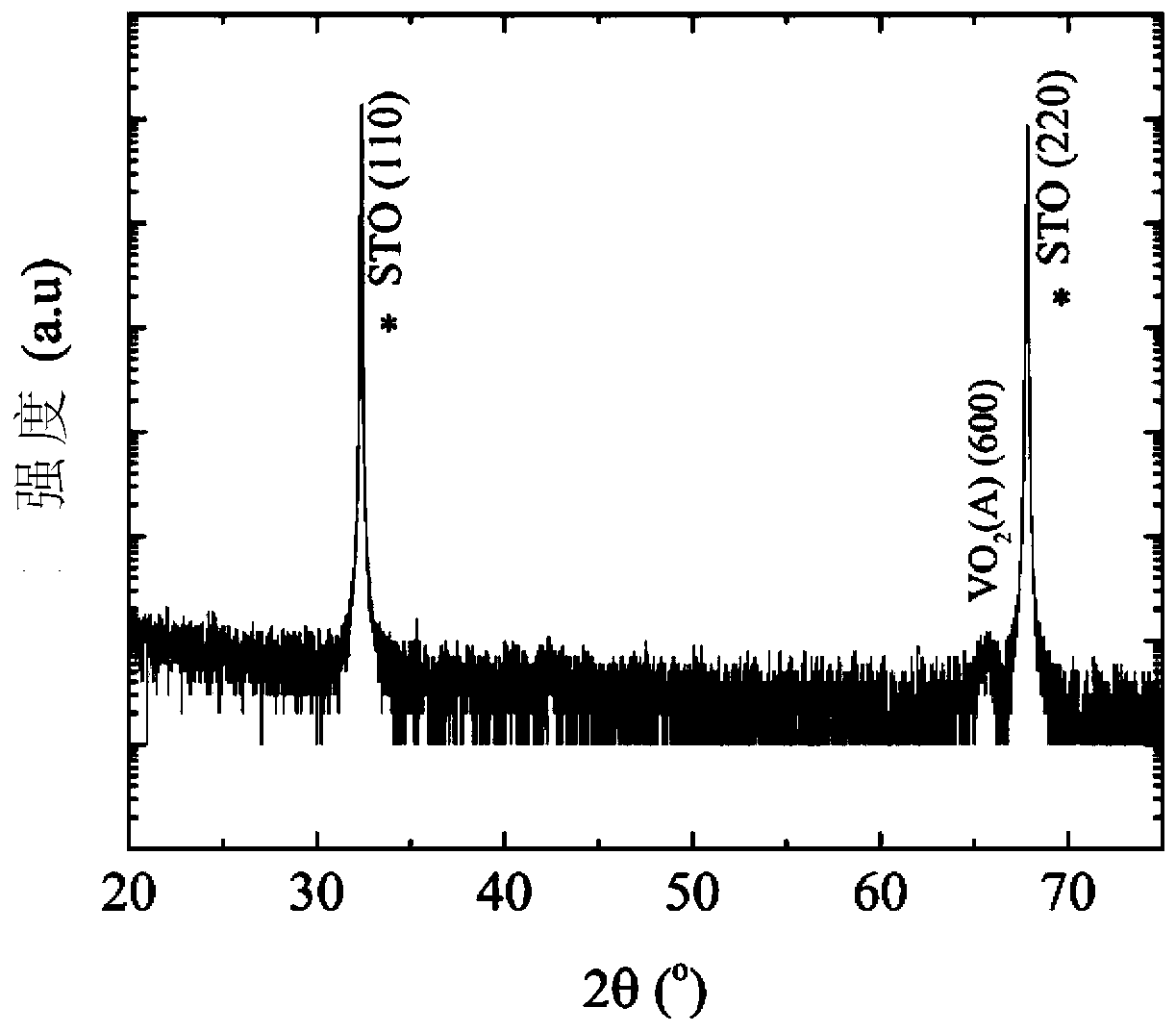
[0026] The obtained film was characterized by X-ray diffraction, and the results are shown in the attached figure 1 . Using X-ray diffraction as parallel light incident mode, θ-2θ scanning. From figure 1 It can be seen that the obtained sample is A-phase vanadium dioxide, and the film epitaxy mode is (100) orientation epitaxy. There are no other impurity peaks in the spectrum except the substrate and phase A vanadium dioxide, which proves that the phase purity of the obtained sample is high.
Embodiment 2
[0028] Vanadium dioxide ceramic target is used, the sputtering gas is argon with a purity of 99.99%, the reaction gas is oxygen with a purity of 99.99%, and the background vacuum is controlled to be 8×10 -5 Pa, deposition temperature 500°C, deposition total pressure 3.0Pa, oxygen partial pressure 5%, sputtering power 70W, sputter vanadium dioxide thin film on (110) surface lanthanum aluminate substrate for 120 minutes. Cool down naturally after sputtering.
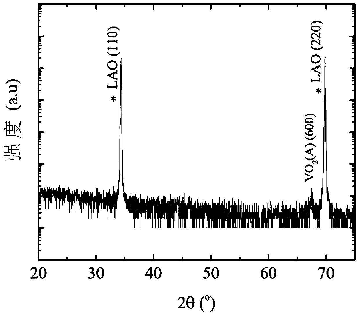
[0029] The obtained film was characterized by X-ray diffraction, and the results are shown in the attached figure 2 . Using X-ray diffraction as parallel light incident mode, θ-2θ scanning. From figure 2 It can be seen that the obtained sample is A-phase vanadium dioxide, and the film epitaxy mode is (100) orientation epitaxy. There are no other impurity peaks in the spectrum except the substrate and phase A vanadium dioxide, which proves that the phase purity of the obtained sample is high.
Embodiment 3
[0031] Vanadium dioxide ceramic target is used, the sputtering gas is argon with a purity of 99.99%, the reaction gas is oxygen with a purity of 99.99%, and the background vacuum is controlled to be 5×10 -5Pa, deposition temperature 200°C, deposition total pressure 1.0Pa, oxygen partial pressure 3%, sputtering power 120W, on (110) surface dysprosium scandate (DyScO 3 ) on the substrate by sputtering vanadium dioxide thin film for 40 minutes. Cool down naturally after sputtering. Characterization of the samples proved that dysprosium scandate (DyScO 3 )(100) direction and VO 2 (A) Phase lattice matching to obtain a phase A vanadium dioxide film.
PUM
 Abstract
Description
Claims
Application Information
 - R&D
- Intellectual Property
- Life Sciences
- Materials
- Tech Scout
- Unparalleled Data Quality
- Higher Quality Content
- 60% Fewer Hallucinations
Browse by: Latest US Patents, China's latest patents, Technical Efficacy Thesaurus, Application Domain, Technology Topic, Popular Technical Reports.
© 2025 PatSnap. All rights reserved.Legal|Privacy policy|Modern Slavery Act Transparency Statement|Sitemap|About US| Contact US: help@patsnap.com


