Semiconductor device and manufacturing method thereof

A semiconductor and device technology, applied in the field of semiconductor devices and their manufacturing, can solve problems such as performance to be improved

Active Publication Date: 2018-03-09
SEMICON MFG INT (SHANGHAI) CORP +1
View PDF4 Cites 3 Cited by
  • Summary
  • Abstract
  • Description
  • Claims
  • Application Information

AI Technical Summary

Problems solved by technology

[0004] However, the performance of the electric programmable fuse device in the prior art needs to be improved

Method used


Image

  • Semiconductor device and manufacturing method thereof
  • Semiconductor device and manufacturing method thereof
  • Semiconductor device and manufacturing method thereof

Examples


Embodiment Construction

[0035] According to the background art, the performance of the electrically programmable fuse device formed in the prior art needs to be improved.

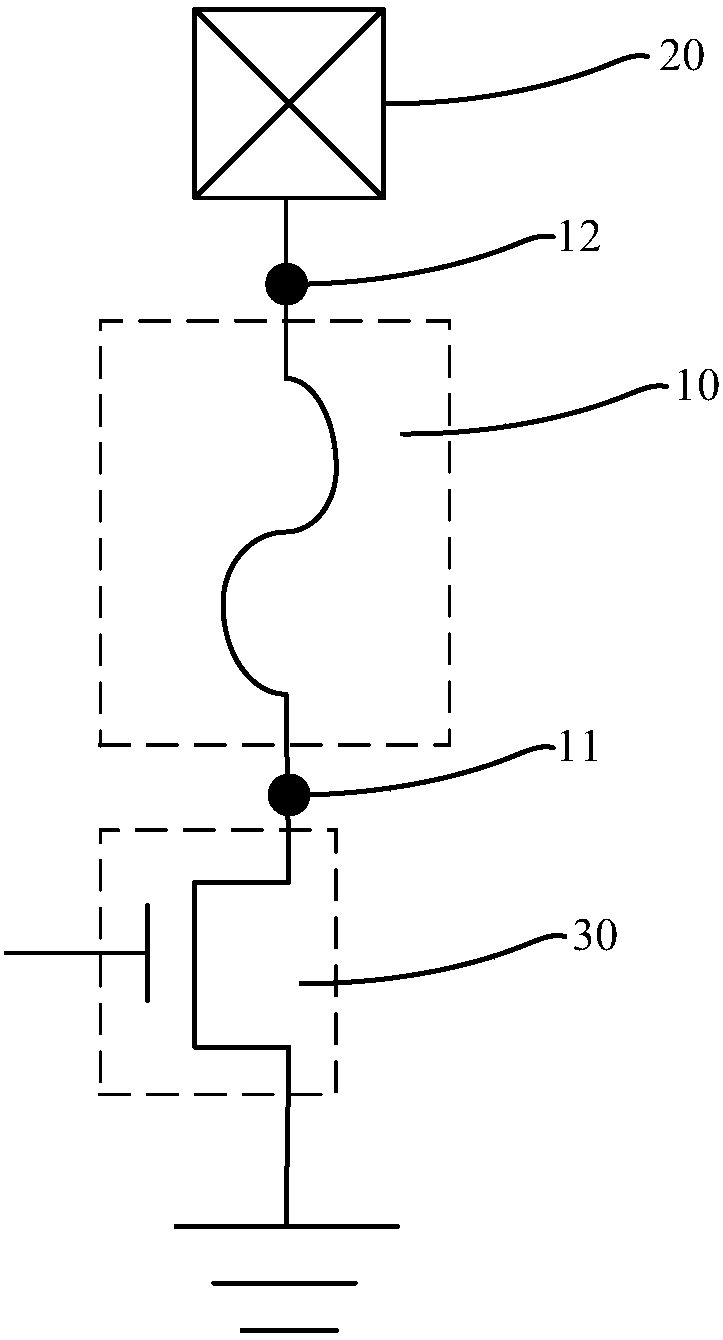
[0036] Now combined with an electric programmable fuse device for analysis, refer to figure 1 , figure 1 It is a schematic structural view of a single unit in an electrically programmable fuse device, which includes: a fuse 10 having a cathode 11 and an anode 12; a welding pad 20 connected to the welding pad 20 The anode 12 of the fuse 10 is connected; the programming transistor 30, the source of the programming transistor 30 is connected to the cathode 11 of the fuse 10, and the drain of the programmable transistor is grounded.

[0037] Wherein, in the layout design of the electric programmable fuse device, the programming transistor 30 and the fuse 10 are arranged side by side.

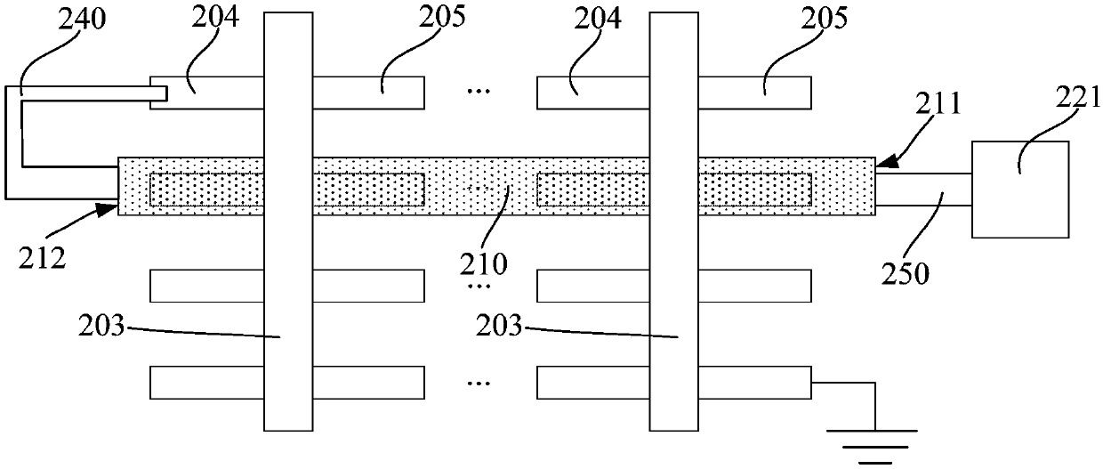
[0038]However, the e-fuse device provided above takes a long time to blow the fuse 10 , so the programming time of the e-fuse device is long and the ...


PUM


Abstract

The invention discloses a semiconductor device and a manufacturing method thereof. The semiconductor device comprises a FinFET device, a Fuse device and a dielectric layer, wherein the FinFET device comprises a base, fin parts protruding against the base, gate structures located on the base and crossing over the fin parts and covering part of top parts and side walls of the fin parts, and a sourceand a drain located in fin parts at two opposite sides of the gate structure; the Fuse device is located right above the FinFET device and has an anode end and a cathode end, the cathode end is electrically connected with the source of the FinFET device, and the anode end is electrically connected with an external liner; and the dielectric layer is located between the FinFET device and the Fuse device. The programming time of the semiconductor device can be shortened, and the programming efficiency is improved.

Description

technical field [0001] The invention relates to the technical field of semiconductor manufacturing, in particular to a semiconductor device and a manufacturing method thereof. Background technique [0002] With the miniaturization of semiconductor technology and the increase of complexity, semiconductor components become more susceptible to various defects or impurities, and the failure of a single wire, diode or transistor often constitutes a defect of the entire chip. In order to solve this problem, A fuse is introduced into the integrated circuit to improve the yield of the integrated circuit. [0003] At present, the fuse structures that are widely used in integrated circuits are Electrically Programmable Fuse Structure (Efuse, Electrically Programmable Fuse Structure), Electrically Programmable Fuse Structure and Complementary Metal Oxide Semiconductor (CMOS, Complementary Metal Oxide Semiconductor) High process compatibility, simple operation, small size and high flex...

Claims


Application Information

Patent Timeline
Patent Type & Authority Applications(China)
IPC IPC(8): H01L29/78H01L27/112
CPCH01L29/785H10B20/20H01L21/823431H01L27/0886H01L23/5256H01L29/7851
Inventor 甘正浩
Owner SEMICON MFG INT (SHANGHAI) CORP
Why Eureka
Try Eureka