Source drain variable-resistance rectangular grid controlled U-shaped channel bidirectional transistor and production method thereof

A rectangular gate, source-drain technology, applied in semiconductor/solid-state device manufacturing, semiconductor devices, electrical components, etc., can solve the problems that the sub-threshold swing cannot be reduced, and ordinary tunneling field effect transistors can only be used as one-way switches.

Inactive Publication Date: 2018-03-09
山东光岳九州半导体科技有限公司
View PDF4 Cites 4 Cited by
  • Summary
  • Abstract
  • Description
  • Claims
  • Application Information

AI Technical Summary

Problems solved by technology

[0007] In order to effectively combine and utilize the advantages of interchangeable source and drain of MOSFETs type devices and the low subthreshold swing swing of ordinary tunneling field effect transistors, solve the problem that the subthreshold swing of MOSFETs type devices cannot be reduced and ordinary tunneling field effect transistors It can only be used as a one-way switch. The present invention proposes a source-drain resistance variable rectangular gate-controlled U-shaped channel bidirectional transistor and its manufacturing method.

Method used


Image

  • Source drain variable-resistance rectangular grid controlled U-shaped channel bidirectional transistor and production method thereof
  • Source drain variable-resistance rectangular grid controlled U-shaped channel bidirectional transistor and production method thereof
  • Source drain variable-resistance rectangular grid controlled U-shaped channel bidirectional transistor and production method thereof

Examples


Embodiment Construction

[0069] The present invention will be further explained below in conjunction with the drawings:

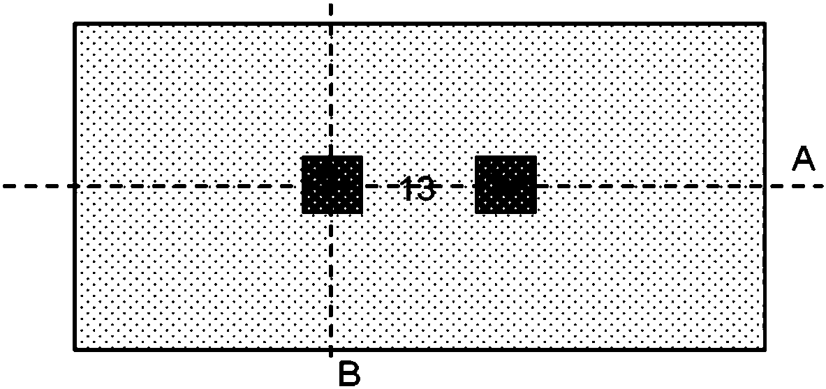
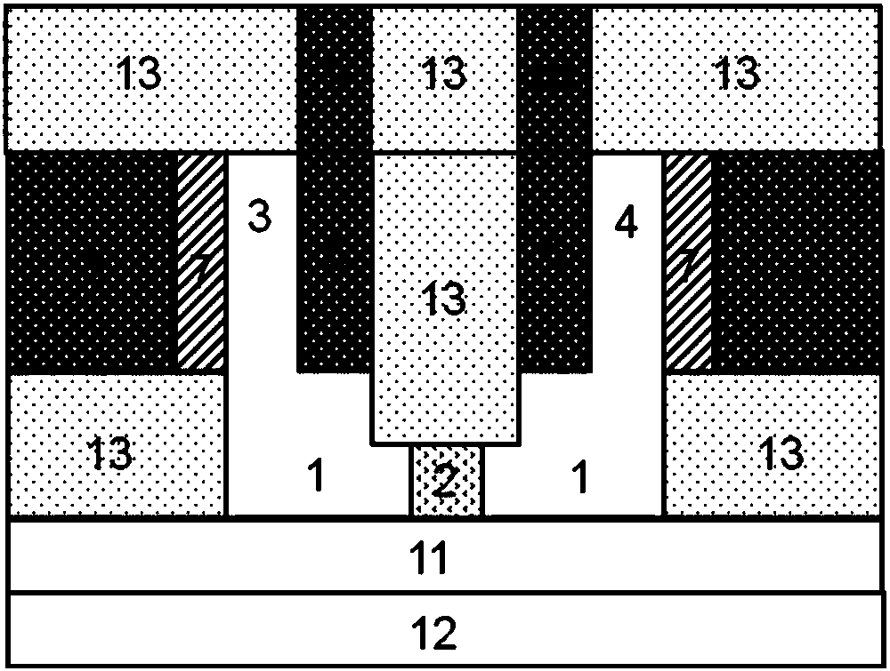
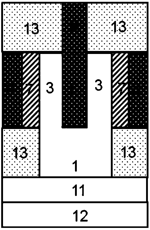
[0070] Such as figure 1 , figure 2 with image 3 As shown, a source-drain resistance variable rectangular gated U-shaped channel bidirectional transistor including a silicon substrate 12 of an SOI wafer is characterized in that: the silicon substrate 12 of the SOI wafer is above the substrate of the SOI wafer Insulating layer 11, above the insulating layer 11 of the substrate of the SOI wafer is a part of the monocrystalline silicon film 1, the heavily doped region 2 and the insulating dielectric barrier layer 13. Among them, the monocrystalline silicon film 1 has an impurity concentration lower than 10 16 cm -3 The single crystal silicon semiconductor material; the heavily doped region 2 is located in the middle part of the bottom of the single crystal silicon film 1, and its doped impurity conductivity determines the conduction type of the device, and its interior is not controlled b...


PUM


Abstract

The invention relates to a source drain variable-resistance rectangular grid controlled U-shaped channel bidirectional transistor and a production method thereof. The element is provided with a rectangular grid electrode, has a transversely symmetrical structural feature, has high grid control capacity and can control a metal source drain interchangeable region as a source region or a drain regionthrough adjustment of source drain interchangeable electrode voltage, and the direction of a tunneling current is changed. The element has the advantages of low static power consumption, small reverse leakage current, high grid control capacity, low subthreshold swing and realization of a bidirectional switch function. Compared with a common MOSFETs-type element, a better switch characteristic isachieved by means of a tunneling effect; compared with a common tunneling field effect transistor, the bidirectional transistor has a source drain interchangeable bidirectional symmetrical switch characteristic; compared with a Schottky barrier transistor, the bidirectional transistor has a better switch characteristic; it is unnecessary to conduct blending in the source and drain regions, a Schottky barrier is easy to form, the rectangular grid electrode can better control the source and drain regions, and thus the bidirectional transistor is suitable for application and popularization.

Description

Technical field [0001] The invention relates to the field of ultra-large-scale integrated circuit manufacturing, in particular to a source-drain resistance variable rectangular gate-controlled U-shaped channel bidirectional transistor with low leakage current suitable for manufacturing low-power integrated circuits and a manufacturing method thereof. Background technique [0002] According to the requirements of Moore's Law, the basic unit MOSFETs of integrated circuits must become smaller and smaller in size. The resulting problem is not only the increase in difficulty in the manufacturing process, but also the various adverse effects caused by the smaller size of the device itself. Highlight. Nowadays, MOSFETs used in integrated circuit design are limited by the physical mechanism of their own current generation during operation, and their sub-threshold swing cannot be lower than 60mV / dec. [0003] Ordinary tunneling field effect transistors use the carrier tunneling mechanism w...

Claims


Application Information

Patent Timeline
Patent Type & Authority Applications(China)
IPC IPC(8): H01L29/78H01L21/336
Inventor 靳晓诗王艺澄刘溪
Owner 山东光岳九州半导体科技有限公司
Why Eureka
Try Eureka