LED epitaxial growth method

A technology of epitaxial growth and growth temperature, applied in the direction of electrical components, circuits, semiconductor devices, etc., can solve the problems of contaminated substrate materials, contaminated substrates, expensive prices, etc., to reduce operating voltage, increase probability, and reduce contact resistance Effect

Active Publication Date: 2018-03-09
XIANGNENG HUALEI OPTOELECTRONICS
View PDF6 Cites 0 Cited by
  • Summary
  • Abstract
  • Description
  • Claims
  • Application Information

AI Technical Summary

Problems solved by technology

However, the In in the ITO film 2 o 3 The price is expensive, the production cost is high, and the In material is toxic, and it is easy to cause harm to the staff during the process of preparing and applying the ITO film. In addition, the atomic mass of Sn and In is large, and it is easy to penetrate into the ITO film during the preparation of the ITO film. Inside the substrate, the substrate material is polluted, especially in the field of liquid crystal displays, the ITO thin film contaminates the substrate most seriously

Method used


Image

  • LED epitaxial growth method
  • LED epitaxial growth method
  • LED epitaxial growth method

Examples


Embodiment 1

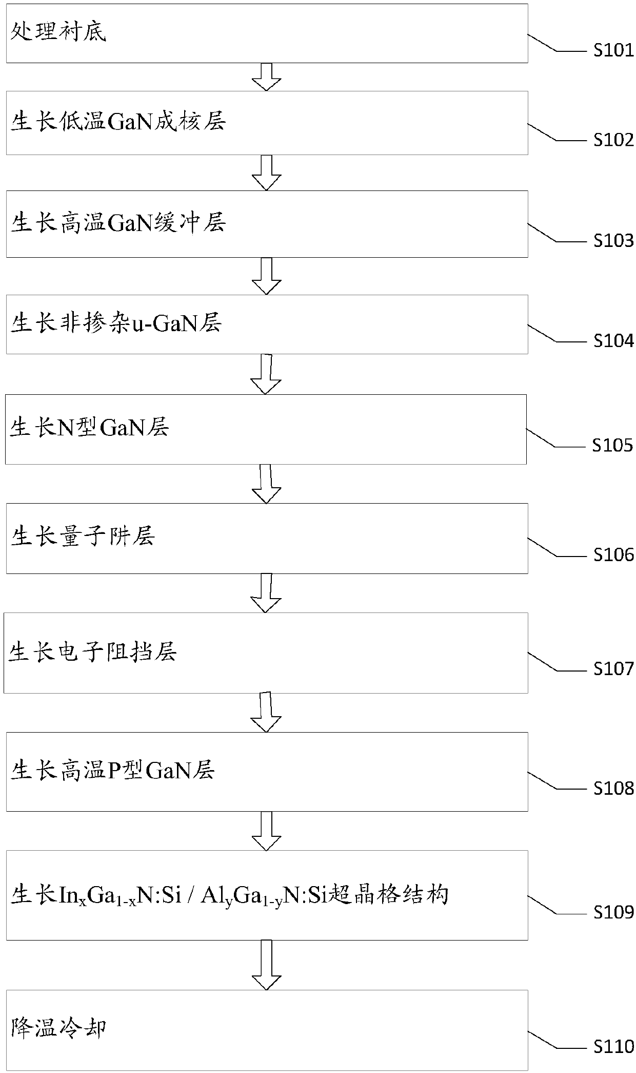
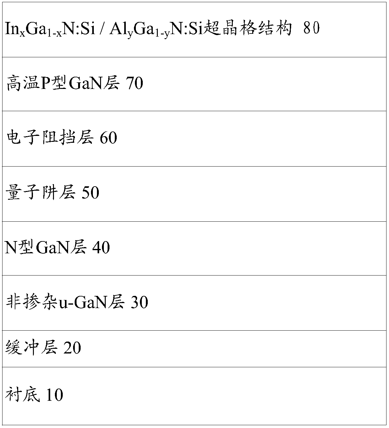
[0047] In Example 1 of the present invention, VEECO MOCVD is used to grow high-brightness GaN-based LED epitaxial wafers. Using high-purity H 2 , high purity N 2 Alternatively, high purity H 2 and high purity N 2 The mixed gas, as a carrier gas, high-purity NH 3 As the N source, the metal-organic source trimethylgallium (TMGa) and the metal-organic source triethylgallium (TEGa) are the gallium source, trimethylindium (TMIn) is the indium source, and trimethylaluminum (TMAl) is the aluminum source , dimethyl zinc (DMZn) as zinc source, N-type dopant as silane (SiH 4 ), the P-type dopant is magnesocene (CP2Mg), the substrate is sapphire, and the reaction pressure is between 100Torr-1000Torr.

[0048] figure 1 It is a method for LED epitaxial growth in Embodiment 1 of the present invention, such as figure 1 As shown, the present invention provides a method for LED epitaxial growth, comprising:

[0049] S101: Treating the substrate; S102: Growing a low-temperature GaN nucl...

Embodiment 2

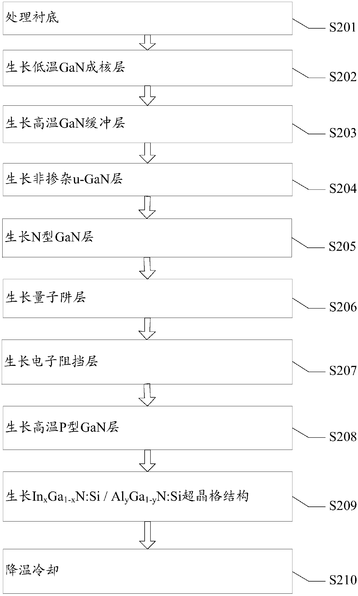
[0057] In Example 2 of the present invention, VEECO MOCVD is used to grow high-brightness GaN-based LED epitaxial wafers. Using high-purity H 2 , high purity N 2 Alternatively, high purity H 2 and high purity N 2 The mixed gas, as a carrier gas, high-purity NH 3 As the N source, the metal-organic source trimethylgallium (TMGa) and the metal-organic source triethylgallium (TEGa) are the gallium source, trimethylindium (TMIn) is the indium source, and trimethylaluminum (TMAl) is the aluminum source , dimethyl zinc (DMZn) as zinc source, N-type dopant as silane (SiH 4 ), the P-type dopant is magnesocene (CP2Mg), the substrate is (0001) plane sapphire, and the reaction pressure is between 100torr and 1000torr.

[0058] image 3 It is a method for LED epitaxial growth in Embodiment 3 of the present invention, such as image 3 As shown, the present invention provides a method for LED epitaxial growth, comprising:

[0059] S201: processing the substrate;

[0060] In some opt...


PUM

PropertyMeasurementUnit
Thicknessaaaaaaaaaa

Abstract

The invention discloses an LED epitaxial growth method, comprising the steps of processing a substrate; growing a low-temperature GaN nucleation layer; growing a high temperature GaN buffer layer; growing a non-doped u-GaN layer; growing a N type GaN layer; growing a quantum well layer; growing an electronic barrier layer; growing a high temperature P type GaN layer; growing InxGa1 xN:Si / AlyGa1 yN:Si superlattice structure, and conducting cooling. The growth of the InxGa1 xN:Si / AlyGa1 yN:Si superlattice structure comprises the steps of adjusting the growth temperature as 750-1050DC, and adjusting the growing pressure as 100 Torr-500Torr. The growth of the InxGa1 XN:Si in thickness of 1nm-5nm comprises the steps of adjusting the growth temperature as 750-1050 DC, and adjusting the growing pressure as 100 Torr-500Torr. The growth of the AlyGa1 yN:Si in thickness of 1nm-5nm comprises the steps of alternatively growing the InxGa1 xN:Si and AlyGa1 yN:Si with the period being 1-10. The invention is advantageous in that through the InxGa1 xN:Si / AlyGa1 yN:Si superlattice structure, the barrier height difference with AZO film material can be adjusted, and contact resistor can be reduced, and work voltage of the LED chip can be decreased, and brightness can be enhanced.

Description

technical field [0001] The invention relates to the field of LED chips, and more specifically, to a method for LED epitaxial growth. Background technique [0002] With the development of semiconductor, computer, solar energy and other industries, transparent conductive oxide (transparent conducting oxide, TCO) thin films are produced and developed. TCO thin films have optoelectronic properties such as wide band gap, high light transmittance in the visible spectrum region and low resistivity. Among them, ITO (In 2 o 3 : Sn) thin film. However, the In in the ITO film 2 o 3 The price is expensive, the production cost is high, and the In material is toxic. In the process of preparing and applying the ITO film, it is easy to cause harm to the staff. In addition, the atomic mass of Sn and In is large, and it is easy to penetrate into the ITO film during the preparation of the ITO film. Inside the substrate, the substrate material is polluted, especially in the field of liqui...

Claims


Application Information

Patent Timeline
IPC IPC(8): H01L33/06H01L33/00
Inventor 林传强徐平
Owner XIANGNENG HUALEI OPTOELECTRONICS
Why Eureka
Try Eureka