radiation detector

A radiation detector and radiation technology, applied in radiation measurement, instrumentation, X/γ/cosmic radiation measurement, etc., can solve problems such as image quality degradation

Active Publication Date: 2020-10-23
KONICA MINOLTA INC
View PDF14 Cites 0 Cited by
  • Summary
  • Abstract
  • Description
  • Claims
  • Application Information

AI Technical Summary

Problems solved by technology

Usually, the scintillator is heated during vapor deposition in the manufacturing process, so there is a problem that the scintillator itself is stressed due to the difference in thermal expansion between heating and cooling, and cracks are generated, resulting in a decrease in image quality. Patent Document 7 does not address such a problem at all. recognize

Method used


Image

  • radiation detector
  • radiation detector
  • radiation detector

Examples


Embodiment

[0190] Hereinafter, the present invention will be described in detail through examples, but the present invention is not limited thereto.

manufacture example

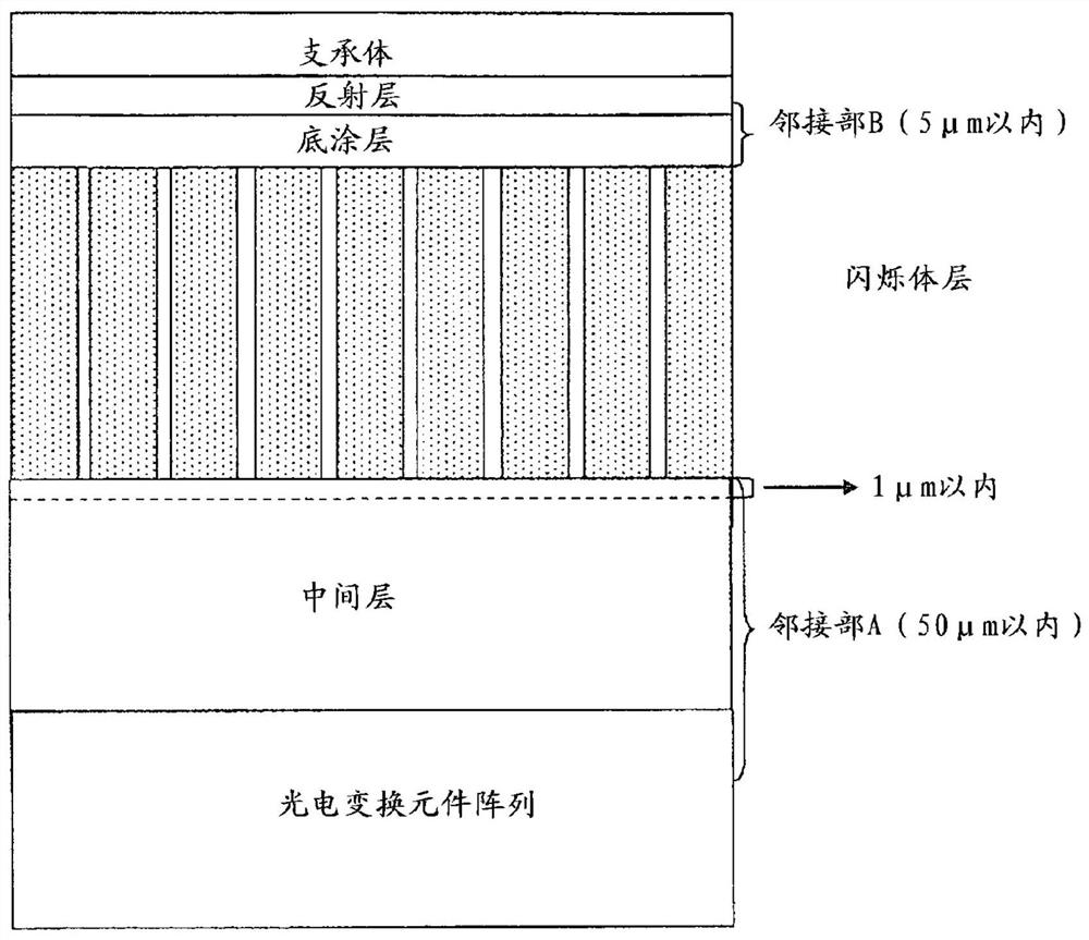
[0192] As the support, a polyimide film (UPILEX-125S, manufactured by Ube Industries, Ltd.) with a thickness of 125 μm was used.

[0193] (production of reflective layer)

[0194] The resin reflection layers of Examples 1 to 6 and Comparative Examples 1 to 5 were coated with titanium oxide dispersed in polyester fiber resin with a thickness of 50 μm.

[0195] In Example 7, silver was sputtered, and in Example 8, aluminum was sputtered to form a reflective layer (100 nm).

[0196] Examples 9 and 10 did not form a reflective layer.

[0197] (Preparation of base coat)

[0198] The SiO of embodiment 1,9,10 and comparative example 2,3 2 The undercoat layer is formed by sputtering of silicon dioxide. The thickness is 100 nm.

Embodiment 2

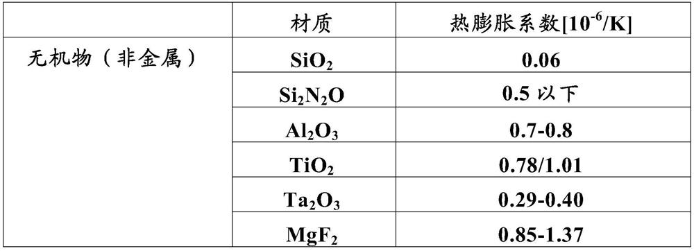
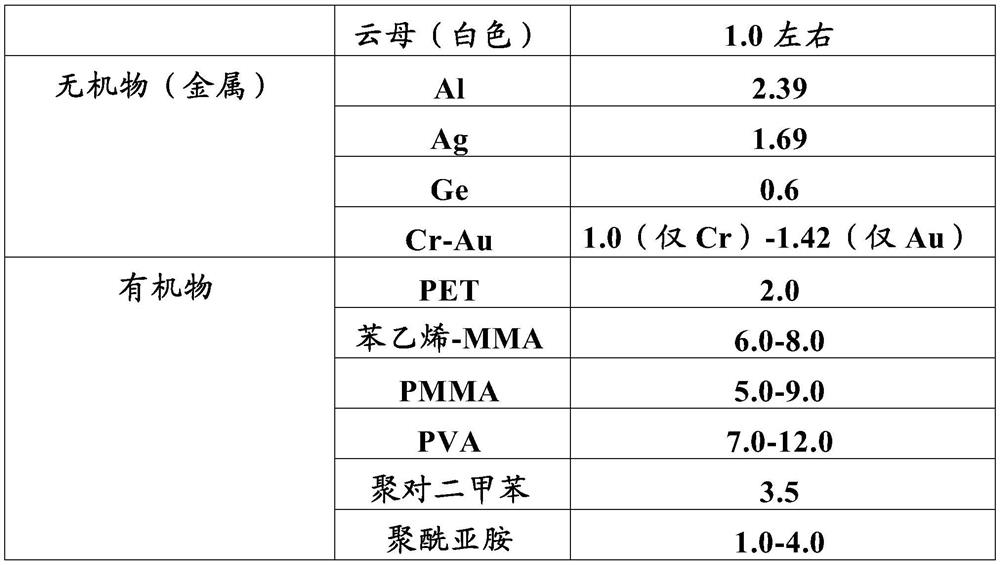
[0199] Example 2 by Al 2 o 3 The bottom coat that constitutes, embodiment 3 and comparative example 5 are made of TiO 2 The base coat that constitutes, embodiment 4 and comparative example 4 are made of MgF 2 The constituting undercoat layer was prepared by applying a dispersion obtained by dispersing these particles in a solvent to a thickness of 50 μm and drying it. As the binder, a binder containing 30% by mass of polyester fiber resin relative to the particles was used.

[0200] Regarding the polyester fiber undercoat layer of Examples 5, 7 and 8, and Comparative Example 1, by dissolving Byron (registered trademark) "200 (type)" (Toyobo Co., Ltd.) in methyl ethyl ketone [MEK] Manufacture: polymer polyester fiber resin), and apply so that the dry film thickness becomes 3 μm to form a primer layer.

[0201] The polymethyl methacrylate (PMMA) undercoat layer of Example 6 was dissolved in methyl ethyl ketone [MEK] and applied so that the dry film thickness would be 3 μm to...


PUM

PropertyMeasurementUnit
thicknessaaaaaaaaaa
emission peakaaaaaaaaaa
thicknessaaaaaaaaaa

Abstract

The present invention provides a radiation image detector, comprising: a photoelectric conversion element array; a scintillator layer; a reflection layer located opposite to the photoelectric conversion element array across the scintillator layer; an undercoat layer existing between the scintillator layer and the reflection layer, and connected to the scintillator layer in an image forming region;and an intermediate layer existing between the photoelectric conversion element array and the scintillator layer, werhein a portion where the distance from the tip of the scintillator layer to the photoelectric conversion element array is within 50 [mu]m is defined as a scintillator adjacent portion A, a position where the distance from the evaporated surface of the scintillator layer to one sideopposite to the photoelectric conversion element array is within 50 [mu]m is defined as a scintillator adjacent portion B, each of the scintillator adjacent portion A and the scintillator adjacent portion B includes one or more kinds of inorganic substances, and a thermal expansion coefficient difference between the substances having the minimum thermal expansion coefficient included in the scintillator adjacent portion A and the scintillator adjacent portion B is 1.5*10<-5>[ / K] or less.

Description

technical field [0001] The present invention relates to a radiation image detector capable of preventing cracks generated in a scintillator layer during heating / cooling of a substrate during vapor deposition of a scintillator layer and suppressing degradation of image quality due to the cracks. Background technique [0002] In recent years, digital radiation image detectors represented by computer radiography (CR: computed radiography) and flat panel detectors (FPD: flat panel detector) can directly obtain digital radiation images, which can be displayed on cathode tubes, liquid crystal panels, etc. The image is directly displayed on the device, so it is widely used in image diagnosis in hospitals and clinics. Recently, a flat panel using a scintillator layer containing cesium iodide (CsI) combined with a thin-film transistor (TFT) has attracted attention as a high-sensitivity X-ray image visualization system. [0003] Attempts have been made to reduce the loss of emitted l...

Claims


Application Information

Patent Timeline
Patent Type & Authority Patents(China)
IPC IPC(8): G01T1/164
CPCG01T1/1645
Inventor 礒田圭冈村真一板屋敬子
Owner KONICA MINOLTA INC
Why Eureka
Try Eureka