Manufacturing method of polysilicon thin film, thin film, transistor, substrate and laser equipment

A manufacturing method and technology of laser equipment, which are applied in the manufacturing of semiconductor devices, electric solid-state devices, semiconductor/solid-state devices, etc. The effect of uneven polysilicon grains

Active Publication Date: 2020-06-23
BOE TECH GRP CO LTD
View PDF4 Cites 0 Cited by
  • Summary
  • Abstract
  • Description
  • Claims
  • Application Information

AI Technical Summary

Problems solved by technology

[0004] The purpose of the technical solution of the present invention is to provide a method for making a polysilicon film, a film, a transistor, a substrate, and a laser device, so as to solve the problem of using the prior art excimer laser annealing to make a low-temperature polysilicon film, resulting in higher surface roughness and poor polysilicon crystal grains. uniform problem

Method used


Image

  • Manufacturing method of polysilicon thin film, thin film, transistor, substrate and laser equipment
  • Manufacturing method of polysilicon thin film, thin film, transistor, substrate and laser equipment
  • Manufacturing method of polysilicon thin film, thin film, transistor, substrate and laser equipment

Examples


Embodiment Construction

[0029] In order to make the technical problems, technical solutions and advantages to be solved by the embodiments of the present invention clearer, the following will describe in detail with reference to the drawings and specific embodiments.

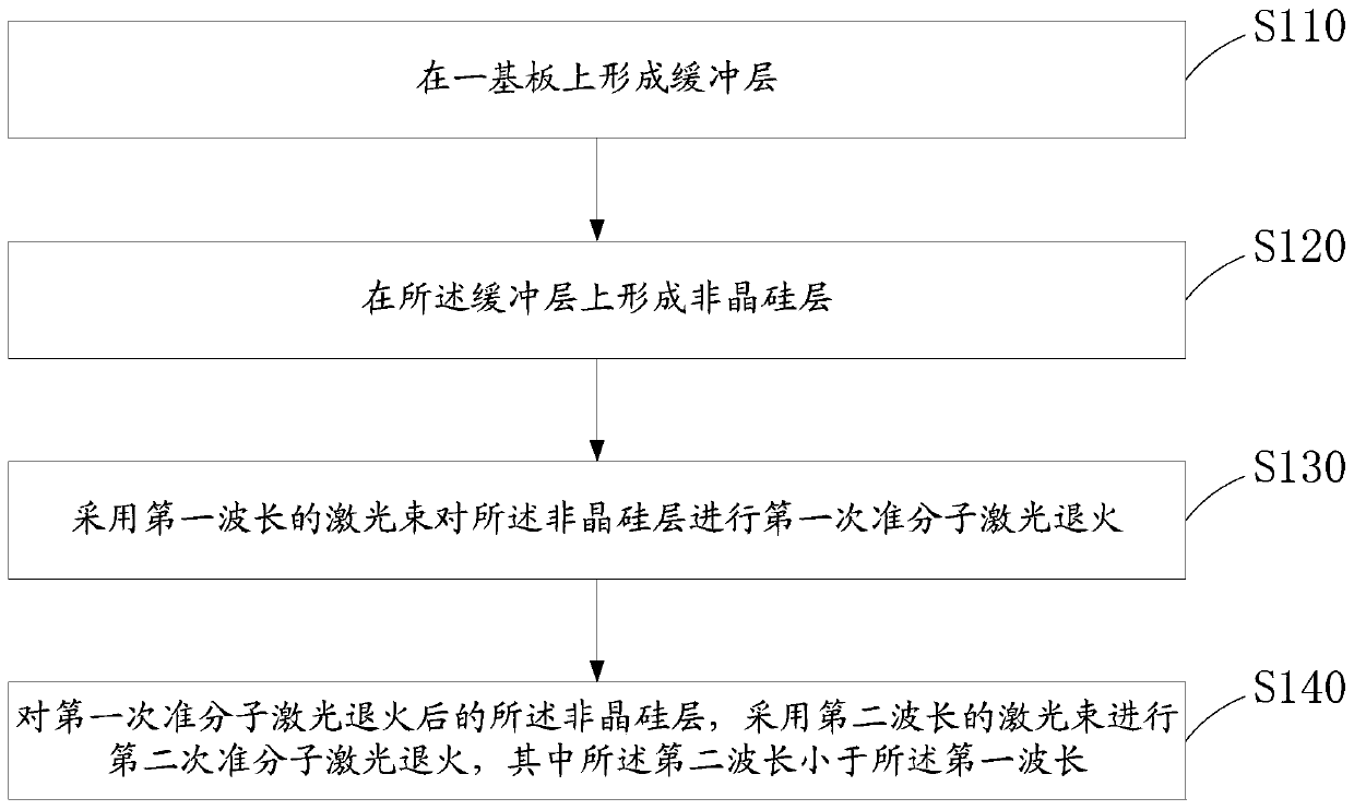
[0030] The manufacturing method of the low-temperature polysilicon film described in the specific embodiment of the present invention, such as figure 1 shown, including steps:

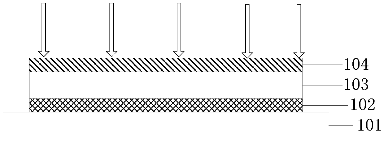
[0031] S110, forming a buffer layer on a substrate;

[0032] S120, forming an amorphous silicon layer on the buffer layer;

[0033] S130, performing excimer laser annealing on the amorphous silicon layer for the first time by using a laser beam of a first wavelength;

[0034] S140, performing a second excimer laser annealing on the amorphous silicon layer after the first excimer laser annealing by using a laser beam of a second wavelength, wherein the second wavelength is smaller than the first wavelength.

[0035] The manufacturing method of the low-tempera...


PUM

PropertyMeasurementUnit
thicknessaaaaaaaaaa
wavelengthaaaaaaaaaa

Abstract

The invention provides a manufacturing method of a polysilicon thin film, a thin film, a transistor, a substrate and a laser device. The method comprises: forming a buffer layer on a substrate; forming an amorphous silicon layer on the buffer layer; performing excimer laser annealing on the amorphous silicon layer for the first time with a laser beam of a first wavelength; The amorphous silicon layer after the sub-excimer laser annealing is subjected to a second excimer laser annealing with a laser beam of a second wavelength, wherein the second wavelength is smaller than the first wavelength. The method of the present invention can solve the problem of high surface roughness and non-uniform polysilicon crystal grains caused by excimer laser annealing in the prior art to produce a low-temperature polysilicon film through two excimer laser annealings with different wavelengths.

Description

technical field [0001] The invention relates to the technical field of low-temperature polysilicon thin films, in particular to a method for manufacturing polysilicon thin films, thin films, transistors, substrates and laser equipment. Background technique [0002] Active-matrix organic light emitting diode (AMOLED) has become the future display due to its advantages of high image quality, short response time of moving images, low power consumption, wide viewing angle and ultra-light and ultra-thin. The best choice for technology. At present, in AMOLED, excimer laser annealing (ELA), solid phase crystallization (SPC) or metal induced crystallization (MIC) is usually used to fabricate the polysilicon layer. Among them, the production of the polysilicon thin film of the active layer of the transistor in the backplane by excimer laser annealing (ELA) process is the only method that has achieved mass production. [0003] Excimer laser annealing (ELA) process is a relatively co...

Claims


Application Information

Patent Timeline
Patent Type & Authority Patents(China)
IPC IPC(8): H01L21/02H01L51/56
CPCH01L21/02532H01L21/02595H01L21/02675H10K71/00
Inventor 田雪雁
Owner BOE TECH GRP CO LTD
Why Eureka
Try Eureka