Bonding encapsulation structure and method suitable for radio frequency MEMS and method

A packaging method and bonding technology, which are applied in the process of producing decorative surface effects, the coupling of optical waveguides, and the assembly of microstructure devices, etc., can solve the problems of not having much advantages, large stress of substrate materials, and high cost. Achieve low cost, high bonding efficiency, and reduce production costs

Pending Publication Date: 2018-03-20
SUZHOU XIMEI MICRO NANO SYST CO LTD
View PDF6 Cites 7 Cited by
  • Summary
  • Abstract
  • Description
  • Claims
  • Application Information

AI Technical Summary

Problems solved by technology

Although the vertical wire interconnection technology realized by TSV technology can greatly increase the density of leads, the cost of TSV technology is relatively high, and it does not have much advantage for devices that do not require high lead density. greater stress

Method used


Image

  • Bonding encapsulation structure and method suitable for radio frequency MEMS and method
  • Bonding encapsulation structure and method suitable for radio frequency MEMS and method
  • Bonding encapsulation structure and method suitable for radio frequency MEMS and method

Examples


Embodiment 1

[0074] A bonding and packaging method suitable for radio frequency MEMS, which is particularly characterized in that it includes the steps of making a package cover, aligning and bonding the package cover with a package substrate, and leading out the wafer lead pads after bonding.

[0075] Specifically, the manufacturing steps of the adopted package cover plate are as follows,

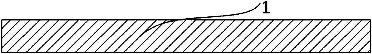
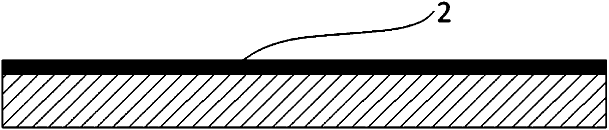
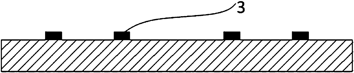
[0076] First, organic materials are spin-coated on a flat high-resistance silicon cover to obtain a high-resistance silicon cover with even distribution of organic materials. During this period, the organic material employed was benzocyclobutene (BCB). Afterwards, photolithography and development are performed on the organic material to form the required bonding pattern. Subsequently, a 520nm Cr layer and a 50nm Au layer were respectively sputtered on the cover plate to form a metal thin film. During this time, the Cr layer was used as an adhesion layer and the Au layer was used as a corrosion stop l...

Embodiment 2

[0084] A bonding and packaging method suitable for radio frequency MEMS, which is particularly characterized in that it includes the steps of making a package cover, aligning and bonding the package cover with a package substrate, and leading out the wafer lead pads after bonding.

[0085] Specifically, the manufacturing steps of the adopted package cover plate are as follows,

[0086] First, organic materials are spin-coated on a flat high-resistance silicon cover to obtain a high-resistance silicon cover with even distribution of organic materials. During this period, the organic material used was polyimide (PI). Afterwards, photolithography and development are performed on the organic material to form the required bonding pattern. Subsequently, a 20nm Cr layer and a 200nm Au layer were respectively sputtered on the cover plate to form a metal thin film. During this time, the Cr layer was used as an adhesion layer and the Au layer was used as a corrosion stop layer. Cr an...

Embodiment 3

[0094] A bonding and packaging method suitable for radio frequency MEMS, which is particularly characterized in that it includes the steps of making a package cover, aligning and bonding the package cover with a package substrate, and leading out the wafer lead pads after bonding.

[0095] Specifically, the manufacturing steps of the adopted package cover plate are as follows,

[0096] First, organic materials are spin-coated on a flat high-resistance silicon cover to obtain a high-resistance silicon cover with even distribution of organic materials. During this period, the organic material employed was epoxy resin. Afterwards, photolithography and development are performed on the organic material to form the required bonding pattern. Subsequently, a 15nm Cr layer and a 150nm Au layer were respectively sputtered on the cover plate to form a metal thin film. During this time, the Cr layer was used as an adhesion layer and the Au layer was used as a corrosion stop layer. Cr a...


PUM

PropertyMeasurementUnit
depthaaaaaaaaaa
depthaaaaaaaaaa
depthaaaaaaaaaa

Abstract

The invention relates to a bonding encapsulation structure and method suitable for radio frequency MEMS. The method comprises the steps that organic materials are spin-coated on an encapsulation coverplate and patterned, then Cr and Au are sputtered, and an encapsulation cover plate with the uniformly distributed organic materials and cavities is obtained by using a method that the cavities are etched with a TMHA solution. The cover plate full of the cavities is made from a high-resistance silicon material, and the cavities are obtained through wet etching by using the TMAH solution. By meansof the encapsulation method, the organic materials can be smoothly distributed in a bonding area, the effective bonding area of wafer-level bonding is increased, and then the airtightness, the reliability and other performance of the product obtained after bonding are improved. A low-temperature bonding technology is adopted to conduct low-temperature encapsulation of a radio frequency device, and while good mechanical strength and airtightness are achieved, the requirements for encapsulating the RF MEMS device which is sensitive to temperature are met.

Description

technical field [0001] The invention relates to a wafer-level packaging structure and a packaging method thereof, in particular to a bonding packaging structure and a method suitable for radio frequency MEMS. Background technique [0002] RF MEMS is an organic combination of microwave radio frequency theory and micromachining technology. It is guided by microwave radiofrequency theory and uses micron-scale micromachining technology to manufacture passive devices. Compared with traditional passive devices, RF MEMS devices not only have excellent microwave performance such as high isolation, low loss, high linearity, low power consumption, and broadband, but also have the characteristics of small size and easy integration. It has extremely high application value in the next generation communication system. However, due to the special structural characteristics of RF MEMS devices, the requirements for packaging performance are extremely strict, which is one of the key areas of...

Claims


Application Information

Patent Timeline
Patent Type & Authority Applications(China)
IPC IPC(8): B81B7/00B81B7/02B81C1/00B81C3/00
CPCB81B7/0032B81B7/02B81C1/00269B81C3/001B81C2203/0118
Inventor 刘泽文杨中宝龚著浩梅剡粼
Owner SUZHOU XIMEI MICRO NANO SYST CO LTD
Why Eureka
Try Eureka