A kind of manufacturing method of high mobility electron transistor

A technology with high mobility and manufacturing methods, which is applied to circuits, electrical components, semiconductor devices, etc., can solve the problems of increasing surface height drop, unfavorable manufacturing process, and increasing the overall thickness of transistors, so as to increase thickness, improve performance, and reduce resistance. Effect

Active Publication Date: 2020-07-17
XIAMEN SANAN INTEGRATED CIRCUIT
View PDF5 Cites 0 Cited by
  • Summary
  • Abstract
  • Description
  • Claims
  • Application Information

AI Technical Summary

Problems solved by technology

Although increasing the thickness of the gate metal deposition can reduce the resistance, it will obviously increase the overall thickness of the transistor and increase the surface height drop, which is not conducive to the subsequent process
Therefore, based on the consideration of size miniaturization, the deposition thickness of gate metal is often limited

Method used


Image

  • A kind of manufacturing method of high mobility electron transistor
  • A kind of manufacturing method of high mobility electron transistor
  • A kind of manufacturing method of high mobility electron transistor

Examples


Embodiment 1

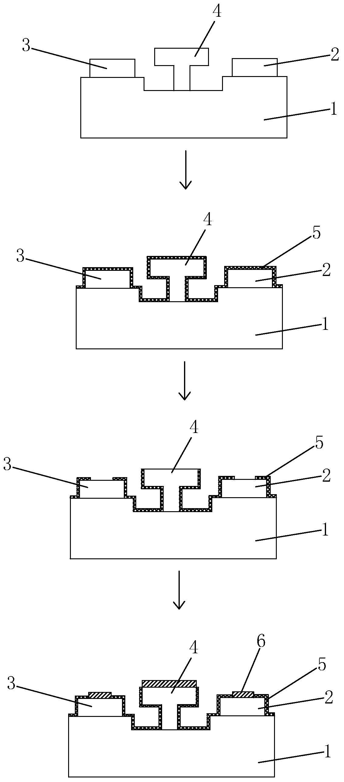
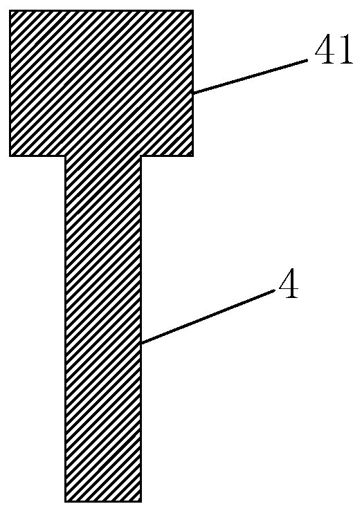
[0026] refer to figure 1 , a kind of manufacturing method of high-mobility electron transistor of embodiment 1, firstly provide the high-mobility electron transistor structure that has finished device manufacturing process, described high-mobility electron transistor structure comprises compound semiconductor substrate 1 and is deposited by metal A source 2, a drain 3 and a gate 4 are formed on a compound semiconductor substrate. The semiconductor substrate 1 can be a group III and V compound semiconductor, such as GaAs, InGaP, InP and the like. The gate 4 is a T-shaped gate structure, and the top line width is greater than the bottom line width. Specifically, the bottom line width is 0.2-0.3 μm, and the top line width is 0.8-1.2 μm. refer to figure 2 , viewed from above, the gate 4 is located between the source 2 and the drain 3 , and its end is expanded to form a lead-out pad 41 . The gate 4 is a Ti / Pt / Au metal composite layer with a thickness of 20-40nm / 20-40nm / 500-700n...

Embodiment 2

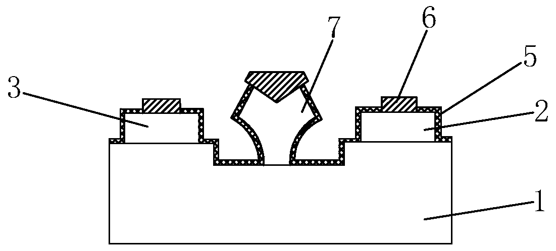
[0032] refer to image 3 The difference between embodiment 2 and embodiment 1 is that the gate 7 has a Y-shaped gate structure, the line width at the bottom is 0.1-0.2 μm, and the line width at the top is 0.7-0.9 μm. The gate 7 is a Ni / Au metal composite layer with a thickness of 10-30nm / 100-300nm, for example, 20nm / 200nm.

[0033] Similarly, during the fabrication of the first metal wiring layer, metal is deposited on the Y-shaped gate with a narrow line width and its lead-out pad at the same time, which increases the thickness of the gate metal layer while realizing the lead-out of the wiring, and reduces the resistance of the gate metal. Floor. Among them, the thickening of the gate metal layer and the metal interconnection are formed in the same metal interconnection process, which is suitable for standard manufacturing processes. While increasing the thickness of the gate metal layer, the overall thickness of the device is not increased, and the large height difference i...


PUM

PropertyMeasurementUnit
thicknessaaaaaaaaaa
thicknessaaaaaaaaaa
thicknessaaaaaaaaaa

Abstract

The invention discloses a manufacturing method of a high-mobility electronic transistor. A protective layer is formed at the surface of a high-mobility electronic transistor structure in which a device process is completed and covers the source, drain and grid electrodes of the structure, holes are etched in the protective layer which covers the source and drain electrodes, the protective layer which covers the grid electrode and a leading-out pad thereof are all etched, and a first metal connecting line layer is deposited. Metal is deposited in the holes of the source and drain electrodes aswell as the leading-out pad of the grid electrode and serves as a connecting line, and metal is also deposited on the grid electrode and serves as a top metal layer of the grid electrode at the same time, so that the thickness of the metal of the grid electrode is increased on the premise that the total thickness is not increased, and the resistance of the grid electrode is reduced. According to the method, only change of a photomask is needed, extra processes are not needed, and the method is suitable for practical production and application of a routine production line.

Description

technical field [0001] The invention relates to a manufacturing process of a semiconductor device, in particular to a manufacturing method of a high-mobility electronic transistor. Background technique [0002] Many parameters on the pseudomorphic High Electron Mobility Transistor (pHEMT) affect the high-frequency response characteristics of the device, among which the gate resistance is an important parameter. It is generally used in high electron mobility transistors used in the manufacture of RF power devices. In order to improve the high-frequency performance of the device, the core is to reduce the gate resistance. The way to reduce the resistance includes increasing the cross-sectional area and increasing the thickness. The current development trend is that the device Highly integrated and miniaturized, therefore, seeking solutions to improve performance and reduce size mergers is of great significance to the development of the industry. [0003] The process used in t...

Claims


Application Information

Patent Timeline
Patent Type & Authority Patents(China)
IPC IPC(8): H01L29/778
CPCH01L29/66431
Inventor 颜志泓魏鸿基
Owner XIAMEN SANAN INTEGRATED CIRCUIT
Why Eureka
Try Eureka