High-EB bipolar semiconductor protection device and manufacturing method thereof
A technology for protecting devices and manufacturing methods, applied in semiconductor/solid-state device manufacturing, semiconductor devices, electric solid-state devices, etc., capable of solving problems such as single protection function
- Summary
- Abstract
- Description
- Claims
- Application Information
AI Technical Summary
Problems solved by technology
Method used
Image


Examples
Embodiment Construction
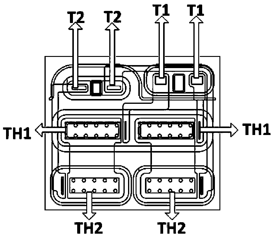
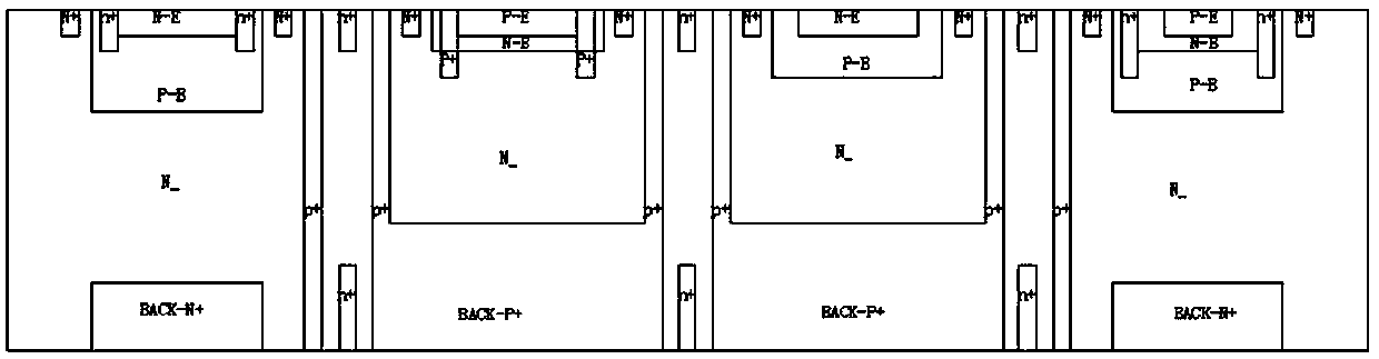
[0033] Such as Figure 1-4 As shown, a high EB bipolar semiconductor protection device includes a chip, two NPN transistors with an N-type silicon wafer substrate are arranged on the upper left of the chip, two PNP transistors are arranged on the lower left of the chip, and the chip Two SCR thyristors arranged up and down are arranged in the middle part, and two TRIAC thyristors arranged up and down are arranged in the right area of the chip.
[0034] A method for manufacturing a high EB bipolar semiconductor protection device, comprising the following steps:
[0035] Step 1: Provide an N-type CZ substrate silicon wafer for double-sided polishing, with a resistivity of 30-35Ω cm and a wafer thickness of 210±5μm;
[0036] Step 2: Perform high-temperature and long-term wet oxygen oxidation on the silicon wafer substrate, T=1150±10°C, t=12h[1h(O2)↑4h wet oxygen+1h(O2)+ 4h wet oxygen+ 2h(O2)+ 4h(N2,O2)↓], oxide layer thickness dsio2≥1.4μm;
[0037] Step 3: P-type partition wa...
PUM
 Abstract
Description
Claims
Application Information
 - R&D
- Intellectual Property
- Life Sciences
- Materials
- Tech Scout
- Unparalleled Data Quality
- Higher Quality Content
- 60% Fewer Hallucinations
Browse by: Latest US Patents, China's latest patents, Technical Efficacy Thesaurus, Application Domain, Technology Topic, Popular Technical Reports.
© 2025 PatSnap. All rights reserved.Legal|Privacy policy|Modern Slavery Act Transparency Statement|Sitemap|About US| Contact US: help@patsnap.com