Composite trench MOS device and manufacturing method thereof

A MOS device and composite technology, applied in semiconductor/solid-state device manufacturing, electric solid-state devices, semiconductor devices, etc., can solve the problems of occupying chip area and cost, occupying silicon surface area, large chip area, etc., and achieve manufacturing cost reduction , high product performance, simple production process

Active Publication Date: 2018-03-30
华羿微电子股份有限公司
View PDF7 Cites 2 Cited by
  • Summary
  • Abstract
  • Description
  • Claims
  • Application Information

AI Technical Summary

Problems solved by technology

The disadvantage is still high cost, high requirements for packaging, and large overall area after packaging
[0006] The third stage is to design and manufacture trench MOSFETs and Schottky diodes in the same chip. The method of processing trench MOSFETs and Schottky diodes is to use partition design and differentiated manufacturing schemes, and realize through wire bonding. Interconnection still occupies a large amount of chip area and cost
Therefore, the disadvantages are always: 1. The Schottky diode structure occupies a large amount of silicon surface area, resulting in large chip area and high cost; 2. The process is complicated, resulting in high manufacturing cost.

Method used


Image

  • Composite trench MOS device and manufacturing method thereof
  • Composite trench MOS device and manufacturing method thereof
  • Composite trench MOS device and manufacturing method thereof

Examples


Embodiment Construction

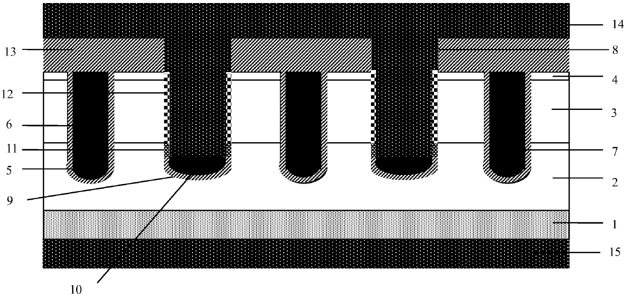
[0052] In order to make the object, technical solution and advantages of the present invention clearer, the present invention will be further described in detail below in conjunction with the accompanying drawings and embodiments. It should be understood that the specific embodiments described here are only used to explain the present invention, not to limit the present invention.

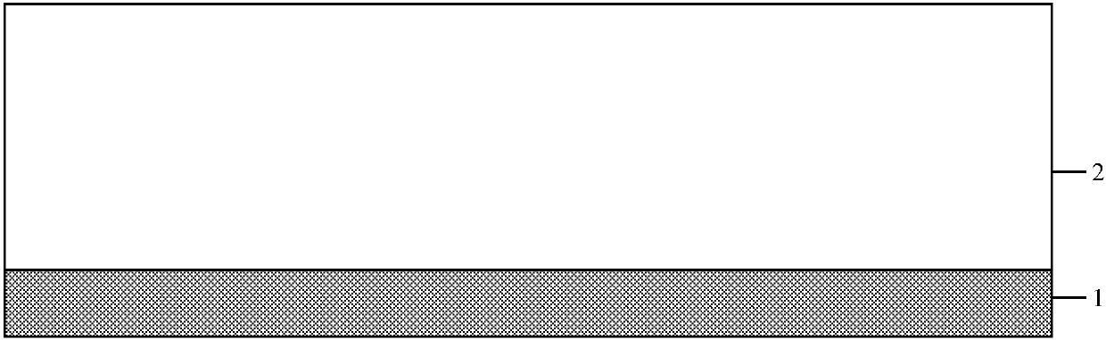
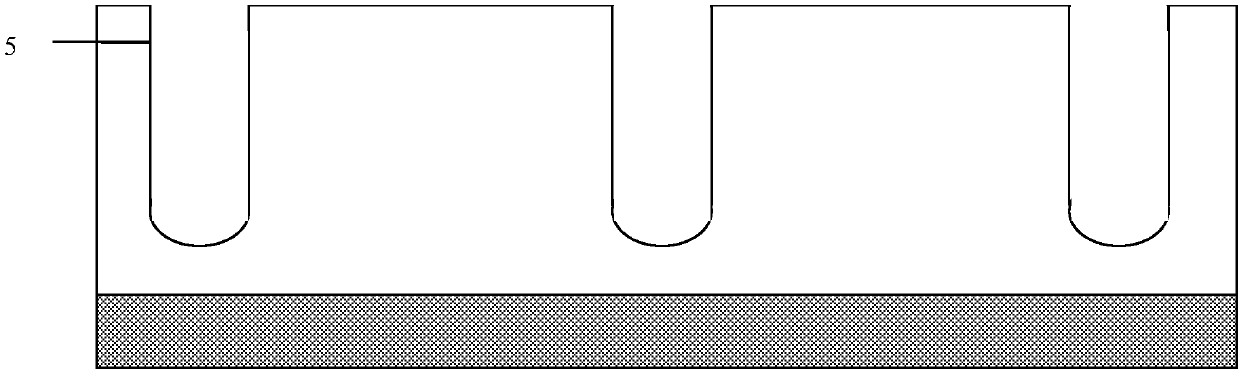
[0053] An embodiment of the present invention provides a composite trench MOS device, such as figure 1 As shown, the device includes a drain region of the first conductivity type, an N+ monocrystalline silicon substrate 1 and an N- epitaxial layer 2 located above the drain region of the first conductivity type, and an N-epitaxial layer located above the N- epitaxial layer 2 The first conductivity type P-type well region layer 3, the second conductivity type source region layer 4 located above the first conductivity type P-type well region layer 3, the second conductivity type source region layer 4 ...


PUM


Abstract

The invention belongs to the technical field of semiconductor power devices and specifically relates to a composite trench MOS device and a manufacturing method thereof. A Schottky diode structure anda TMBS structure are integrated in a contact hole of each trench MOSFET unit cell, Schottky contact is formed at a side wall of a contact hole of the trench MOSFET unit cell, a switching loss is reduced and spike voltage and spike current are suppressed, and a reverse recovery characteristic is improved. The TMBS structure is formed at the bottom of the contact hole, a balanced electric field canbe formed in the device, the breakdown characteristics of the device are improved, thus while the performance of the device is improved, a silicon surface area is effectively saved, and the cost of achip is reduced. The composite trench MOS device has the advantages of a simple manufacturing process, low cost, a novel structure and high product performance and reliability, peak voltage and peakcurrent of trench MOSFET device reverse recovery can be effectively suppressed, and the voltage withstanding performance of the device is improved.

Description

technical field [0001] The invention relates to the technical field of semiconductor power devices, in particular to a composite trench MOS device structure and a manufacturing method thereof. Background technique [0002] With the continuous and rapid development of my country's economy, energy consumption is also increasing year by year, especially in the context of global warming, "low-carbon economy" has gradually become a global hotspot, so energy conservation has become one of my country's basic national policies. The new power electronic devices play a particularly important role in it. Among them, the trench MOS device is a semiconductor device with rapid development and good market prospects. It has fast switching speed, high input impedance, good thermal stability and strong reliability. It has a wide range of applications in the fields of computers, communication equipment, power supply circuits of general office equipment, and automotive electronic circuits. [...

Claims


Application Information

Patent Timeline
Patent Type & Authority Applications(China)
IPC IPC(8): H01L27/06H01L29/06H01L29/78H01L21/336H01L21/8249
CPCH01L27/0629H01L29/0623H01L29/66666H01L29/7827H01L21/8249Y02B70/10
Inventor 袁力鹏徐吉程范玮
Owner 华羿微电子股份有限公司
Why Eureka
Try Eureka