AlGaN-based solar-blinded ultraviolet avalanche heterojunction photoelectric transistor detector and fabrication method thereof

A phototransistor, ultraviolet avalanche technology, applied in photovoltaic power generation, semiconductor devices, circuits, etc., can solve the problems of slow response speed, easy failure, and high avalanche operating voltage

Inactive Publication Date: 2018-03-30
SUN YAT SEN UNIV
View PDF3 Cites 16 Cited by
  • Summary
  • Abstract
  • Description
  • Claims
  • Application Information

AI Technical Summary

Problems solved by technology

[0004] For the existing AlGaN-based APDs, the leakage current is large under high reverse bias voltage, the avalanche excess noise is large (the avalanche is jointly triggered by electrons and holes), the avalanche operating voltage is high, and the dislocation density in the epitaxial layer of the material is high. The problem of easy failure under avalanche breakdown working conditions; HPT has problems such as low weak light detection

Method used


Image

  • AlGaN-based solar-blinded ultraviolet avalanche heterojunction photoelectric transistor detector and fabrication method thereof

Examples


Embodiment Construction

[0026] The accompanying drawings are for illustrative purposes only, and should not be construed as limitations on this patent; in order to better illustrate this embodiment, certain components in the accompanying drawings will be omitted, enlarged or reduced, and do not represent the size of the actual product; for those skilled in the art It is understandable that some well-known structures and descriptions thereof may be omitted in the drawings. The positional relationship described in the drawings is for illustrative purposes only, and should not be construed as a limitation on this patent.

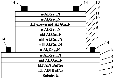
[0027] like figure 1 As shown, this method is suitable for making an AlGaN-based sun-blind ultraviolet avalanche heterojunction phototransistor detector. The inductive photoelectric gain can achieve high photoelectric gain at a lower operating voltage, and at the same time avoid the difficult problems of increased leakage current (dark current) and reduced reliability of AlGaN photod...


PUM

PropertyMeasurementUnit
Thicknessaaaaaaaaaa
Thicknessaaaaaaaaaa
Thicknessaaaaaaaaaa

Abstract

The invention relates to the technical field of a semiconductor ultraviolet photoelectric detector, in particular to an AlGaN-based solar-blinded ultraviolet avalanche heterojunction photoelectric transistor detector and a fabrication method thereof. The AlGaN-based solar-blinded ultraviolet avalanche heterojunction photoelectric transistor detector comprises a substrate, wherein an unintentionally-doped low-temperature AlN buffer layer, an unintentionally-doped high-temperature AlN buffer layer, an unintentionally-doped Al<m>Ga<1-m>N window layer, an n-type Al<m>Ga<1-m> layer, an n-type Al<n>Ga<1-n>N constituent slowly-changing layer, an unintentionally-doped AlGa<1-a>N absorption multiplication layer, an unintentionally-doped AlGa<1-b>N absorption multiplication layer, an unintentionally-doped Al<c>Ga<1-c>N absorption multiplication layer, an Mg-doped p-type Al<x>Ga<1-x>N layer, an unintentionally-doped Al<x>Ga<1-x>N layer, an n-type Al<y>Ga<1-y>N constituent slowly-changing layer, an n-type Al<z>Ga<1-z>N layer and an n-type ohmic contact electrode are sequentially grown on the substrate by a metal organic chemical vapor deposition epitaxial growth method (or a molecular beam epitaxial growth method), and the n-type ohmic contact electrode is finally obtained by deposition of a device process.

Description

technical field [0001] The invention relates to the technical field of semiconductor ultraviolet photodetectors, more specifically, to an AlGaN-based sun-blind ultraviolet avalanche heterojunction phototransistor detector and a preparation method thereof. Background technique [0002] In recent years, with the development of information technology, people have more and more diversified means of capturing and detecting surrounding environment information. The demand for ultraviolet photodetectors is also increasing. [0003] At present, the common ultraviolet photodetectors on the market are mainly Si-based photodiodes and vacuum electron photomultiplier tubes equipped with filters. Ultraviolet photodetectors based on Group III nitride semiconductors (including binary compounds GaN, AlN, ternary compounds AlGaN, InGaN, AlInN and quaternary compounds AlInGaN) have direct band gaps due to the semiconductor material system, and the forbidden bands of their multiple compounds T...

Claims


Application Information

Patent Timeline
IPC IPC(8): H01L31/11H01L31/18
CPCH01L31/11H01L31/1848Y02E10/544Y02P70/50
Inventor 江灏欧杨辉邱新嘉
Owner SUN YAT SEN UNIV
Why Eureka
Try Eureka